The specific width of the induced channel per unit area of the structure, the efficiency of technological shunting of the emitter of a parasitic thyristor, the specific capacity of the gate (the specific charge of the gate required for switching the device), as well as the ability to ensure the accumulation of excess charge carriers in a lightly doped area adjacent to emitter depend on the design of the MOSFET structure and adjacent emitter semiconductor layers.
Planar Cell
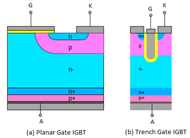
The first commercial IGBTs were manufactured using a planar cell structure.
On the one hand, the popularity of the planar cell is due to the good compatibility of its manufacturing technology with a well-developed route for manufacturing CMOS chips with a polysilicon gate. On the other hand, such a cell provides an acceptable combination of characteristics of the MOSFET structure, hidden gate wiring, reliable shunting of the emitter of a parasitic thyristor.
Trench Cell
The use of mesorelief in the form of rectangular or V-shaped grooves allows getting a very compact cell design. The channel here is formed on the sidewall of the groove, which makes it possible to significantly reduce the size of the p-part of the unit cell. A planar cell size of the p-part of the cell is 15-30 microns, and for a trench cell, it is 5-10 microns.
Accordingly, it is possible either to increase the channel width by increasing the cell density, which is effective for low-voltage IGBTs, or to increase the size of the near-surface n-region, which is useful for high-voltage structures, i.e., in any case, to obtain an additional reduction in the voltage drop in the on-state compared to a similar structure with a planar cell.
This is why trench IGBT is a better choice: as a rule, these are devices with the lowest voltage drop for their class. However, it has the increased capacity of the gate and possible problems with limiting the short circuit current.
IEGT Cell
Further development of the trench IGBT design with the accumulation of excess electron-hole plasma in the emitter region is the IEGT (Injection Enhanced Gate Transistor) structure proposed by Toshiba.
In IEGT, the effect of accumulation of excess electron-hole plasma (p-i-n effect) is due to the introduction of additional empty cells into the structure that do not contain n-regions. The effect of reducing the voltage drop is about 0.5-1.0 V compared to a structure with the densest arrangement of MOSFETs.

In such a device there is also the possibility of including a thyristor structure in the current flow, the n-emitter of which is formed by an inverse layer formed by a MOSFET structure over an empty p-region.
CSTBT Cell
A more radical technical solution that allows implementing the p-i-n effect in the structure of the IGBT trench has been proposed by Mitsubishi Electric under the name of CSTBT – Carrier Stored Trench-Gate Bipolar Transistor.
In this device, the effect of accumulation of excess electron-hole plasma is due to the introduction of an additional thin n’-layer into the structure, while a p-i-n structure appears, connected in series with the MOSFET structure. Calculations show that such a modification of the structure makes it possible to reduce the residual voltage drop by 1.5-2 V and obtain a residual voltage drop of about 3 V on crystals with a voltage of 4500 V.
The disadvantage of this design is its technological complexity. The additional n’-layer is adjacent to the high-voltage p-n junction, therefore, in order not to worsen the reverse voltage, the total number of donor impurity atoms in this layer should not exceed (5-7)x1011 cm-2. On the other hand, the maximum volume concentration of donors should be about 1×1016 cm-3 or more, which is necessary to effectively reduce the residual voltage drop. Thus, the thickness of the additional layer should be less than a micron, which is difficult to implement, even with the use of epitaxial technology, given a large number of subsequent heat treatments on the route of the formation of the MOS structure.
SPT+ Enhanced Planar Cell
An additional barrier n’-layer, similar to the one introduced in CSTBT, can also be formed in the IGBT planar cell.
Calculations and experiments have shown, however, that it is much more difficult for such a structure than for CSTBT to maintain a high blocking voltage. Studies have shown that a significant enhancement of the p-i-n effect can be achieved by applying not a continuous barrier n’-layer, but local n’-regions covering the p-region of the cell from the sides. The introduction of these regions leads to an increase in the proportion of the structure area occupied by a conditional p-i-n diode and a decrease in the area of a bipolar transistor with an unsaturated collector p-n junction.
It is much easier to maintain a high blocking voltage on such a structure. The energy loss during turn-off, with a reasonable approach to the design of the semiconductor structure, is possible to keep almost at the level of a standard IGBT similar in blocking voltage, since most of the additional charge of excess carriers is removed from the drift layer at the stage of the turn-off delay. Such modification allows reducing the voltage drop for high-voltage planar IGBTs by 1-1.5 V.
The disadvantage of the design, as with the previous solution, is the technological complexity. Additional n-regions are subject to requirements similar to those for CSTBT. Planar IGBTs with such a structure are produced by Hitachi Energy (former ABB Semiconductors) under the commercial name SPT+. In this solution, the effect is achieved by introducing additional n’-regions surrounding the MOSFET cells.
Learn more about power semiconductors in Power Semiconductors section of my Marketing Psycho blog. And if you are interested in power semiconductors market news, you can always subscribe to my Power Semiconductors Weekly updates.
Power Semiconductors Weekly is a Marketing Psycho weekly podcast covering the latest news from power semiconductors industry. Delivered to you every Tuesday by Alexey Cherkasov, Power Semiconductors Weekly brings you the most interesting events in the world of power semiconductors and power electronics. Subscribe to Power Semiconductors Weekly and watch it on YouTube every Tuesday.
If you prefer a monthly update about the world of power semiconductors delivered to your e-mail address, please, subscribe to Marketing Psycho Power Semiconductors newsletter.