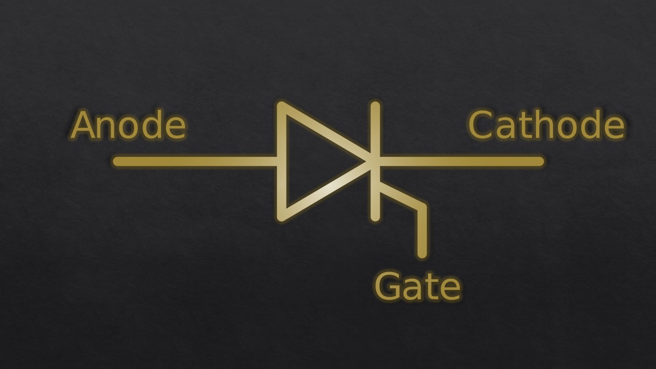
Power semiconductor thyristor is a semiconductor device with four layers of alternating p- and n-type materials. It acts exclusively as a bistable switch, conducting when the gate receives a current trigger, and continuing to conduct until the voltage across the device is reversed biased, or until the voltage is removed (by some other means).
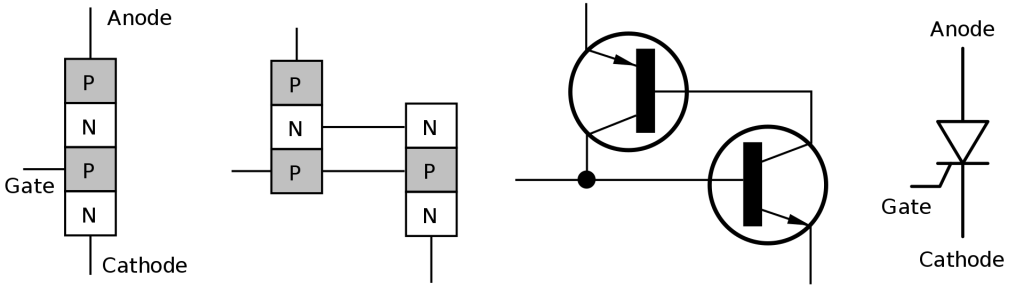
The semiconductor structure of the thyristor has four layers with different types of conductivity: n-emitter, p-base, n-base, p-emitter. These layers are separated by three p-n junctions: the cathode emitter p-n junction is located between the n-emitter and the p-base, the anode emitter p-n junction is between the p-emitter and the n-base, the collector p-n junction is between the p-base and n-base.
The physics of the processes in this semiconductor structure is such that the application of a positive potential to the anode compared to the cathode leads to the occurrence of a current-voltage characteristic with a section of negative differential resistance.
Semiconductor Element Design of Power Semiconductor Thyristor
In a power semiconductor thyristor, usually the most lightly doped high-resistance layer is the n-base, the space charge region of high-voltage collector and anode p-n junctions expand into this layer when forward and reverse voltages are applied in the off state (blocking voltages).
The gate is usually attached to the p-base and is located on the cathode side of the semiconductor. To do this, an n⁺-emitter layer is not formed on a part of the cathode surface, and these p-type areas coming to the surface are called p-type control regions.
The thyristor structure has several important additional elements.
Shunting Cathode Emitter
The shunt elements are made in the form of local p-type regions extending onto the cathode surface and having a common metallization with the n⁺-emitter. Shunts are implemented to guarantee a reduction of the gain factor of the n-p-n component transistor, which is necessary to ensure a high value of the switching voltage of the thyristor, as well as to increase noise immunity and improve some dynamic characteristics.
Branched Gate
Initially the gate current switches a thyristor on only in a relatively narrow of 100-500 μm wide region topologically adjacent to the edge of the control p-region and the gate. It is caused by the finite value of the lateral propagation of the gate current in the semiconductor structure.
Since the area of the semiconductor structure can be very large, the problem arises how to switch on the entire area of the thyristor in an acceptable short time. This problem is solved by the implementation of a branched gate, the topology of which is chosen in such a way as to reduce the propagation time of the on state over the entire area to a reasonable value.
Auxiliary Thyristor
The presence of a branched gate in the semiconductor structure requires an increase in the gate current. The typical gate current required to switch the thyristor structure on evenly along the entire perimeter of the gate is about 1 A per 1 cm of the length of the gate.
Thus, to switch a thyristor on with a branched gate, pulses of gate current with an amplitude of tens or even hundreds of amperes may be required, which greatly complicates the thyristor control unit. To avoid this, an additional auxiliary thyristor structure is introduced.
This auxiliary thyristor is integrated into a common four-layer structure and has a common anode with the main thyristor, but its own gate, and its cathode is connected to the metallization of the branched gate of the main thyristor. The total area of the cathode and the perimeter of the gate of the auxiliary thyristor is much smaller than that of the main one.
The external terminal of the gate of the entire thyristor is connected to the metallization of the gate of the auxiliary thyristor, so when switching this element on first, it does not require high gate current to switch it on. The anode current of the switched-on auxiliary thyristor is supplied to the branched gate of the main thyristor and switches the main structure on.
Semiconductor Element Periphery Area
Similar to power semiconductor diodes, profiling of the edge bevel is most often used to prevent surface breakdown of high-voltage p-n junctions of the power semiconductor thyristor. Since the thyristor has two high-voltage p-n junctions, the bevel profile is more complex than that of a diode.
In semiconductor structures with asymmetric p-n junctions, forward and reverse bevels are distinguished depending on whether the part with a reduced volume has a higher or lower dopant concentration, respectively.
Effective protection against surface breakdown for forward and reverse bevels is achieved at different values of the angle α: for a forward bevel, this angle should be as small as possible, for the reverse bevel, values less than 40-50° are sufficient. Therefore, in order to minimize the size of the peripheral area, the bevel for thyristor structures is usually formed in two stages: the angle α1 is 20-40°, and the angle α2 is 1-3°.
Find more information about power semiconductors in Power Semiconductors section of the website.