Besides the standard design, solder bond, and other already covered in my blog power semiconductor modules, there exist many types of the specific power semiconductor devices.
Modules with Partial Pressure Contact Technology
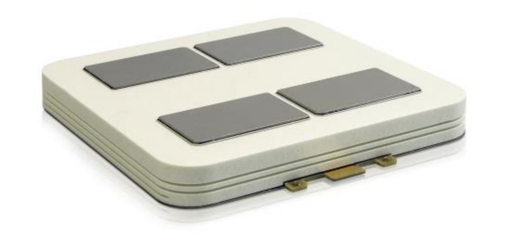
The principal distinguishing feature of the modules with partial pressure contact technology is the design without a baseplate, in which the DCB is mounted directly on the heatsink.
Semiconductor chips, similar to the modules of standard design, are soldered on a ceramic board, while wiring from the upper contact pads is carried out with aluminum wires. To achieve uniform pressure of a thin ceramic board to the heatsink over its entire area, the module package is made in the form of a special support structure with evenly distributed protrusions that rest against the ceramics and provide it a uniformly distributed clamping force.
The positive aspects of the described basic design are clear. First of all, this is the absence of a ceramics/baseplate junction, which ensures the cycling resistance. Secondly, it is the absence of the baseplate itself, the contribution of which to the thermal resistance becomes noticeable if composite materials are used in accordance with ceramics according to the coefficient of linear thermal expansion. Thus, both an increase in power cycling resistance and a decrease in thermal resistance are achieved, compared with the standard design.
The advantages of the design also include a relatively low weight, as well as the possibility of placing all the elements of the module on one large ceramic board, which increases manufacturability. For standard design modules the dimensions of ceramics are limited by inconsistency in the coefficient of linear thermal expansion with the baseplate even if composite materials are used for its production.
The main disadvantage is the complexity of installation by the end customers when installed in the power conversion equipment. The fragility of the ceramic board makes it necessary to impose very strict requirements on the flatness of the heatsink surface, the thickness and uniformity of the heat-conducting paste layer, and the assembly conditions.
Since meeting these harsh conditions causes difficulties for the end customers, many manufacturers of power semiconductor devices are producing these modules already in the form of power units integrated with heatsinks, where the module is placed on the heatsink either directly by the manufacturer or in its technical support offices.
The disadvantage of the design is also the low heat capacity of the ceramic layer separating the semiconductor chip from the contact layer of the paste, which has the worst thermal conductivity in the entire heat-conducting package. As a result, in the transition process, the thermal resistance at the initial stages increases significantly compared to the standard design modules where heat is initially accumulated by a massive baseplate.
The disadvantages also include difficulties when soldering large semiconductor chips on thin ceramics. The local bending of ceramics resulting from the difference in the coefficient of linear thermal expansion worsens the heat removal from the chip.
As a result, manufacturers are switching from soldering to low-temperature diffusion welding of chips using nanostructured silver-containing paste – sintering.
StakPak Press-Pack Modules
Hitachi Energy (ex ABB Semiconductors) developed highly reliable modules of the StakPak series with completely pressurized chips. The modules are used to complete the high-voltage converter equipment of the power grid industry.
StakPak is a family of high-power insulated gate bipolar transistor (IGBT) press-packs and diodes in an advanced modular housing that guarantees uniform chip pressure in multiple-device stacks.
Since IGBTs feature multiple parallel chips, there is a challenge – with conventional press-packs – in assuring uniform pressure on all chips. This problem was solved with a new patented spring technology.
The StakPak, optimized for series connection, features a modular concept based on sub-modules fitted in a fiberglass reinforced frame, which allows a flexible realization of a range of products for different current ratings and IGBT/diode ratios.
Advantages of the design:
- Exceptionally high cycle resistance, due to the absence of solder joints
- Design for series assembly into high-voltage stacks
- High electrodynamic resistance
In case of a breakdown, the module is guaranteed to go into a state of short circuit without the occurrence of an arc, the punctured module can be permanently located as part of a working stack, i.e., it can conduct the operating current for a long time.
Disadvantages of the design:
- Unsealed package
To reduce the negative influence of the environment on chips during long-term operation, the company has developed and applies special metallization of the contact pads. To stabilize the properties of the contacts, multilayer metallization was applied: AlSi-Ti-Ni-Ag. The AlSi layer gives the contact the softness necessary for reliable clamping, the upper layers protect against corrosion. The protection of the chip periphery is also enhanced by SIPOS and Si₃N₄.
- Uninsulated baseplate
These disadvantages are rather conditional, since the design concept outlined above fundamentally allows both the use of an isolated baseplate and multi switch configurations. A specific StakPak series is simply designed for the complete set of high-voltage stacks of electric power conversion equipment, where switches with uninsulated baseplates are required.