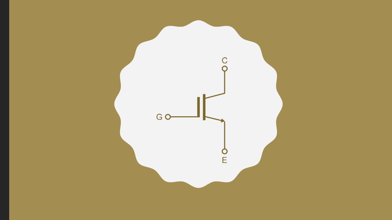
IGBT or Insulated Gate Bipolar Transistor is a fully controllable power semiconductor switch with bipolar conductivity and MOSFET control. The IGBT structure is similar to the structure of a DMOS transistor, with one significant exception. Instead of a drain contact n-layer in the MOSFET, an injecting emitter layer of p-type conductivity is formed here. As a result, when the device is operating in a conductive state (with a formed channel in the MOSFET structure), nonequilibrium excess holes are injected from the emitter layer into a high-resistance drift layer, the charge of which is compensated by nonequilibrium excess electrons.
The excess electron-hole quasi electron neutral plasma thus accumulated in the drift layer reduces the electrical resistance of the layer. The so-called bipolar conduction mechanism is implemented, characteristic of a bipolar p-n-p transistor, which is an integral part of the resulting semiconductor structure (p-emitter layer, n-drift layer (n-base), p-regions of the vertical MOSFET structure).
The gate current of this bipolar transistor is delivered through the channel of the MOSFET structure. Thus, in the on-state, a functional hybrid of bipolar and MOSFET transistors is realized, with the transmission of current occurring as in a bipolar transistor, and control as in a MOSFET. The operation of the device in the off-state corresponds to the operation of a bipolar p-n-p-transistor with a break in the base circuit.

In addition to the bipolar p-n-p-transistor, there is also a parasitic p-n-p-transistor in the IGBT structure, formed by the n- and p-regions of the MOSFET structure and the drift n-layer. They form a parasitic thyristor together with the p-n-p-transistor. The switching of this thyristor leads, as a rule, to irreversible destruction of the structure. Constructive and technological measures must be taken to bypass the emitter junction of the parasitic transistor.
Main Characteristics of IGBT
The IGBT system of characteristics is in many ways close to that for MOSFETs. The current-voltage characteristic in the off-state corresponds to the current-voltage characteristic of the reverse-biased collector p-n junction of IGBT. It is usually characterized by the maximum allowable collector-emitter voltage Vce and the leakage current Ice corresponding to this voltage. Conditions for measuring these characteristics are some specified often negative non-locking gate voltage, Ice measurements are usually carried out for the maximum permissible temperature. Often these measurements are carried out with a short-circuited gate, then the ‘s’ symbol is added to the designations: Vces, Ices.
The current-voltage characteristic in the on-state is characterized by the values of the collector-emitter saturation voltage Vcesat at a specified value of the gate voltage and collector current. The characteristics of the linear approximation of the current-voltage characteristic are also often introduced: cutoff voltage and dynamic resistance. The limiting characteristic of the on-state is the maximum allowable collector current Ic.
Collector current dependence at the constant collector-emitter voltage on the gate voltage is described by the transient characteristic of IGBT. The current-voltage characteristic family gives the most complete picture, both in the field of operating currents and for the collector current limitation area, at various gate voltages.
Characteristics of the gate are usually given as the maximum allowable gate-emitter voltage Vge corresponding to the maximum allowable gate-emitter leakage current (Ige). Additionally, the value of the gate-emitter threshold voltage for the specified values of collector current and collector-emitter voltage (VGE(th)) is given as well.
Typical values of the gate-emitter and gate-collector capacitance. The gate capacitance of the MOSFET structure, due to the Miller effect, strongly depends on the gate-emitter voltage, especially during the transition of the structure from a non-conducting to a conducting state and vice versa. Therefore, the volt-coulomb characteristic of the gate is important. This is the dependence of the gate charge Qg on the gate-emitter voltage under specified conditions in THE collector-emitter circuit. Knowing this dependence, it is easy to calculate what charge in the gate circuit will be required to switch the device.
The turn-on dynamics are characterized by the turn-on time of IGBT ton. It is the time interval from the moment the voltage pulse is applied to the gate until the collector current increases or the collector-emitter voltage decreases to a specified value.
The turn-on time is divided into two phases – the delay time tdon and the rise time tr. The boundary between these two components of the turn-on time is determined at the beginning of a sharp increase in collector current or the beginning of a drop in collector-emitter voltage up or down to the specified values. The power losses in the switching transition process are characterized by the switching energy Eon – the integral of the power loss during the turn-on time.
It should be noted that the switching process of IGBT is very fast, and it is often artificially slowed down by introducing some resistance into the gate circuit, slowing down the process of its recharge. At the same time, the rise phase increases in duration, and the IGBT, which is on, limits the rise of the collector current. The value of Eon in this mode increases significantly, however, the soft switching of IGBT allows for the safe reverse recovery of the freewheeling diode working in conjunction with IGBT in autonomous voltage inverters with a bridge circuit.
The turn-off dynamics are characterized by the IGBT toff turn-off time. This is the time interval from the moment the gate voltage begins to decrease until the collector current drops to a specified value. The turn-off time is divided into two phases – the delay time ts and the collector current fall time tf. The boundary between these two components of the turn-off time is determined by the beginning of the collector current decline to a specified value. Power losses in the transient turn-off process are characterized by Eoff – the integral of the power loss during the turn-off time.
The characteristics of the turn-off time are given, as a rule, for the mode simulating the operation of IGBT in a bridge voltage inverter with an inductive load, i.e., in the most complex circuit version for turning-off. The characteristic of the safe operation area during switching is the maximum permissible pulsed collector current IcM, switching of which is possible when turning on and off in the modes described above.
Learn more about power semiconductors in Power Semiconductors section of my Marketing Psycho blog. And if you are interested in power semiconductors market news, you can always subscribe to my Power Semiconductors Weekly updates.
Power Semiconductors Weekly is a Marketing Psycho weekly podcast covering the latest news from power semiconductors industry. Delivered to you every Tuesday by Alexey Cherkasov, Power Semiconductors Weekly brings you the most interesting events in the world of power semiconductors and power electronics. Subscribe to Power Semiconductors Weekly and watch it on YouTube every Tuesday.
If you prefer a monthly update about the world of power semiconductors delivered to your e-mail address, please, subscribe to Marketing Psycho Power Semiconductors newsletter.