The first diode elements, which can be conditionally referred to as power semiconductor diodes, were created based on a copper – copper oxide rectifying contact in the 1920s. The reverse voltage of one diode element did not exceed 8 V, however, it was possible to connect the elements in series. The permissible current ranged from several hundred milliamps to several amperes.
In the 1930s, selenium-based rectifiers were created, which became a real element base for power rectifiers of that time and were mass-produced by a number of companies in the USA and Europe. Since the 1950s, the development of power semiconductor diodes based on germanium and somewhat later silicon began in the world. Those diodes already had reverse voltages from tens to several hundred volts and current up to tens of amperes.

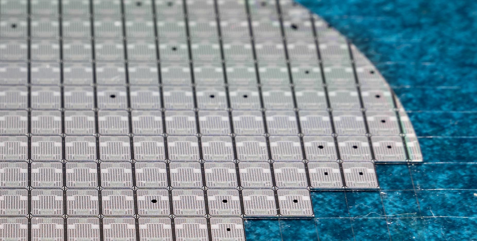
During 1960-1970, silicon technology became dominant in the production of power semiconductors. Diodes were no exception, and up to now they are produced mainly of silicon and are developing in terms of increasing voltage, current, and improving frequency and pulse characteristics.
Since the 1990s, there has been a fairly rapid development of power semiconductor diodes using wide bandgap semiconductor materials, primarily Schottky diodes using silicon carbide. However, due to their high cost, the use of these diodes is still quite limited, and there is no changing dominant diode technology yet.
Power Semiconductor Diodes with P-N Junction
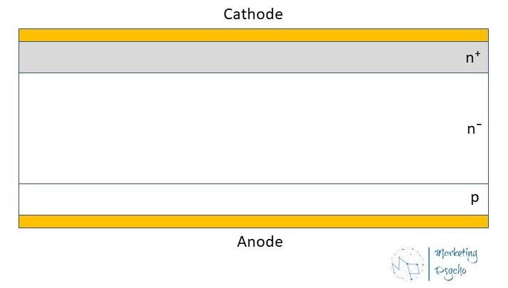
The most widely used diodes in power electronics are diodes with p-n junction. A characteristic feature of a power diode with p-n junction is the presence of at least one lightly doped high-resistance layer between the p-n junction and the surfaces of the structure (anode and cathode).
Schottky Diodes
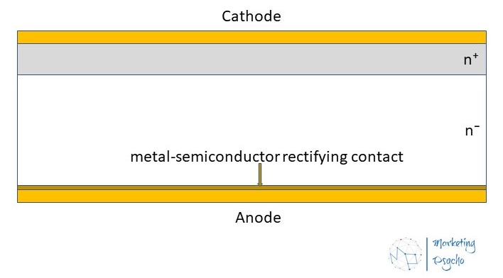
A Schottky diode, as well as a power semiconductor diode with p-n junction, contains a lightly doped high-resistance layer necessary to provide a high blocking voltage, as well as a heavily doped n⁺-layer adjacent to it from the cathode side, providing a low-resistance contact. However, unlike a diode with a p-n junction, the semiconductor structure does not contain p-layers. The rectifying function in the Schottky diode is performed by the metal-semiconductor anode contact.
Thus, the Schottky diode is a semiconductor device with unipolar conductivity, which explains its advantages and disadvantages in comparison with a power diode with a p-n junction.
During its operation, there is no accumulation of nonequilibrium excess electron-hole pairs in the lightly doped layer of the Schottky diode structure, therefore, the resistance of this layer does not decrease with an increase of direct current. Thus, it is possible to obtain an acceptably low forward voltage drop only with a sufficiently small thickness of the n⁻-layer, which imposes significant restrictions on the amount of permissible reverse voltage.
Thus, for silicon-based Schottky diodes, the maximum blocking voltage does not exceed 1000 V, while the permissible forward current density is an order of magnitude lower than that of a diode with a p-n junction designed for the same reverse voltage.
The absence of accumulation of excess electron-hole pairs has a positive consequence. Due to this, the Schottky diode has an exceptionally low loss energy during the transition from a conducting state to a blocking one. Thus, the frequency characteristics of a Schottky diode in comparison with a diode with a p-n junction significantly benefit.
To a large extent, the use of wide bandgap semiconductor materials in Schottky power diodes allows to smooth out the conflicting ratio of forward and reverse voltages, while maintaining high frequency characteristics.