
The main purpose of modification of IGBT deep semiconductor layers is the same as that of other types of bipolar power semiconductor devices. It is to obtain an optimal combination of the voltage drop in the on-state and the switching loss energy (the lowest possible values of both) at the maximum or set value of the blocking voltage. Currently, there are three main structural and technological varieties of deep IGBT layers.
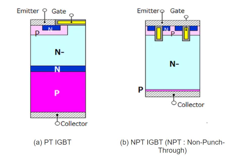
Punch-Through Technology
IGBT structures are formed on epitaxial substrates. They consist of the initial highly doped p⁺-type wafer, a buffer thin n’-layer is formed on it from the planar side, and then a thicker drift n⁻-layer. On the surface of this high-resistance layer, a MOS structure is formed in the form of a regular grid of elementary cells.
The main problem of the punch-through IGBT is technological. The epitaxial layers have a significantly higher defect rate than substrates cut from a single-crystal silicon ingot manufactured using advanced modern technology, for example, float growth followed by neutron doping.
This creates a significant problem with the yield of suitable crystals, especially crystals with an area over 0.5 cm2. The defectiveness of the epitaxial high-resistance layer increases sharply with an increase in its thickness over 80-100 microns, which limits the maximum punch-through IGBT voltage. As a rule, it is not higher than 1700 V.
Non Punch-Through Technology
IGBT structures are formed on the substrates of high-resistance float or neutron doped silicon. A lower injecting p-n junction is formed on the non-planar side of the substrate, and a MOS cell is formed on the planar side.
The use of a low-defect initial substrate made it possible to dramatically increase the size of the crystal. Today, widely used high-current IGBT crystals from the leading manufacturers of power semiconductors have sizes of 10-15 mm, and the maximum sizes of the crystals used reach up to 20-25 mm.
The width of the drift high-resistance n⁻-layer in the non punch-through IGBT is significantly larger than that allowed for the punch-through structures since the restriction of the propagation of the space charge region of the high-voltage p-n junction by the buffer n’-layer is not provided here. Therefore, the voltage drop in the on-state for this type of crystals is usually the largest in comparison with analogs of the other two types.
However, this increase in voltage in the on-state is not so great, since the lifetime of carriers in the drift layer can be increased, and if the current gain coefficients are equal, for example, in comparison with the punch-through structure, the increase in voltage drop will not be significant.
At the same time, the accumulated charge of the excess electron-hole plasma will increase, which can lead to an increase in energy loss during turn-off. However, the power loss largely depends on the nature of the distribution of excess charge carriers over the thickness of the structure and on the injection coefficient of the lower p-n junction. Using these two factors, it is possible in the non punch-through structure to significantly limit the increase in losses during turn-off.
An advantage of the non punch-through technology is a positive temperature coefficient of voltage drop. In addition, these devices, as a rule, have high resistance to soft switching modes, when the IGBT forms a soft current rise front corresponding to the soft current drop front in the diode of the adjacent module, which is necessary to protect this diode. Non punch-through structures have a fairly soft current drop during turn-off and are least likely to enter the high-frequency generation mode, in comparison with IGBT of other types.
Due to these properties, non punch-through IGBTs remain quite popular for use in equipment, despite the availability of advanced FS or SPT technology.
Field-Stop or Soft Punch-Through Technology
This is a logical extension of non punch-through technology. Just as in the non punch-through, IGBT structures are formed on substrates of high-resistance float or neutron doped silicon. MOS cells are formed on the planar side of the substrate. On the non-planar side of the substrate, however, not only the lower injecting p-n junction is formed, but also the buffer n’ layer.
The technology combines all the technological advantages of the non punch-through with the ability to make a device with a minimum thickness of a high-resistance and n⁻-layer and thus minimize the voltage in on-state.
Unlike punch-through, here the corresponding layers are formed by diffusion, so there are quite wide possibilities for controlling the concentration profile of dopant impurities in these layers. This makes it possible to flexibly control the gain of the p-n-p transistor and avoid problems typical for the punch-through structures during turn-off.
Control of the injection coefficient of the lower p-n junction allows not only to minimize power losses during turn-off but also to obtain a positive temperature coefficient of voltage drop, even for structures with an extremely thin drift n⁻-layer.
Thus, field-stop or soft punch-through technology, especially combined with any of the advanced MOS cell designs described, makes it possible to obtain IGBT crystals with the best combination of basic characteristics to date at a moderate price.
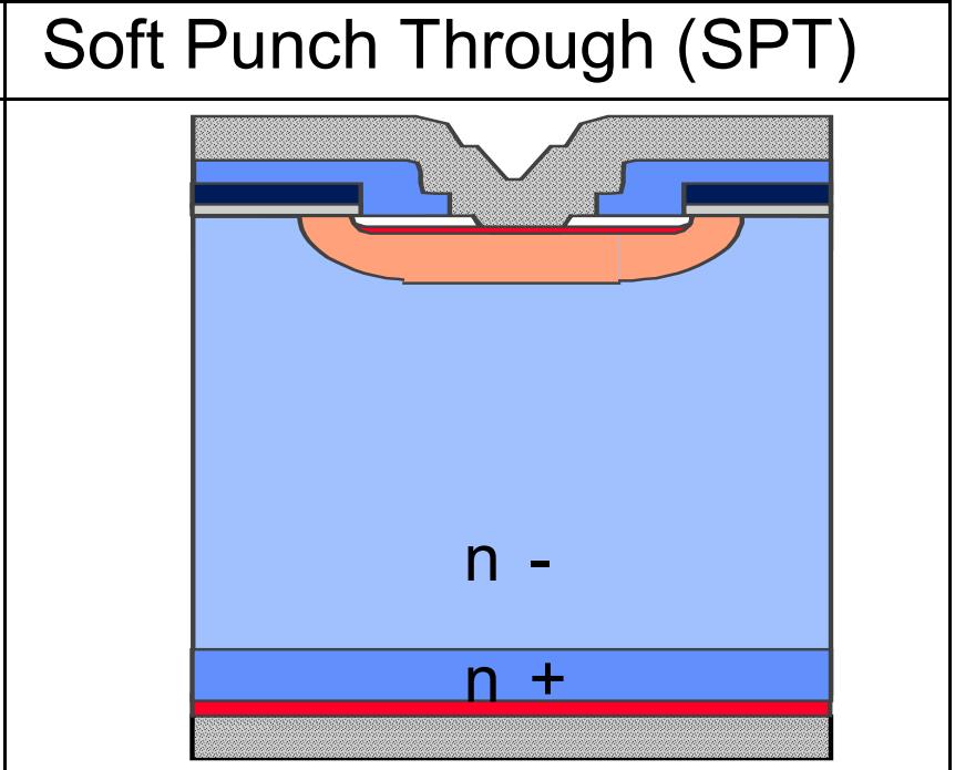
One of the most serious problems of the field-stop or soft punch-through IGBT can happen during turn-off. The presence of a lightly injecting lower p-n junction, which is mandatory to reduce the power losses during turn-off, as well as a fairly powerful buffer n’-layer with a short lifetime of charge carriers can lead to depletion of the reserve of the excess electron-hole plasma in the drift layer and an abnormally fast current drop at the tail.
In the process of a turn-off, the edge of the space charge region of the high voltage p-n junction moves deep into the structure, its position and speed of movement are determined by the instantaneous values of the voltage, the rate of its change, as well as the density of the currents of holes and electrons that create an additional charge in the space charge region. In the process of its expansion, the space charge region captures from the quasi-electroneutral part of the n⁻-layer, which creates a hole current in the structure.
The electron current in the space charge region occurs only in dynamic avalanche breakdown modes, which for IGBTs operating at operating current densities, as a rule, less than 100 A/cm2, are usually uncharacteristic or do not lead to large avalanche currents. Thus, the current of holes in the space charge region usually determines the total current of the structure. If the edge of the space charge region in its movement suddenly falls into a layer where the concentration of electron-hole pairs is reduced, then this leads to an abnormal decrease in current.
Learn more about power semiconductors in Power Semiconductors section of my Marketing Psycho blog. And if you are interested in power semiconductors market news, you can always subscribe to my Power Semiconductors Weekly updates.
Power Semiconductors Weekly is a Marketing Psycho weekly podcast covering the latest news from power semiconductors industry. Delivered to you every Tuesday by Alexey Cherkasov, Power Semiconductors Weekly brings you the most interesting events in the world of power semiconductors and power electronics. Subscribe to Power Semiconductors Weekly and watch it on YouTube every Tuesday.
If you prefer a monthly update about the world of power semiconductors delivered to your e-mail address, please, subscribe to Marketing Psycho Power Semiconductors newsletter.