Power Semiconductors Weekly Vol. 24
Renault Group and STMicroelectronics Enter Strategic Cooperation on Power Electronics
Renault Group and STMicroelectronics announced a strategic cooperation on the design, development, manufacturing, and supply to Renault Group of STMicroelectronics’ products and related packaging solutions for the power electronics systems of battery-operated and hybrid vehicles. These technologies will have significant impacts on electric vehicles’ driving range and charging by reducing power losses and improving efficiency, which will result in lower battery costs, more kilometers per charge, shorter charging time and reduced user-cost.
Renault Group and STMicroelectronics will work together with the objective of improving the power performance of Renault’s Group’s applications for electric and hybrid vehicles, based on STMicroelectronics’ wide bandgap semiconductor technologies and products. The companies will collaborate on the development of efficient, rightsized, and modular components based on the understanding of Renault Group’s technology needs for Silicon Carbide (SiC) devices, Gallium Nitride (GaN) transistors, along with related packages and modules. As Renault’s key innovation partner, STMicroelectronics will benefit from significant volumes guaranteed for the annual usage of these power modules and transistors from 2026-2030.
II-VI Incorporated Introduces Heated Ion Implantation Foundry Services for 150 mm Silicon Carbide Wafers
II‐VI Incorporated, a leading global provider of foundry ion implantation services and support to the microelectronics industry, announced the introduction of heated ion implantation foundry services for 150 mm silicon carbide (SiC) wafers.
The growing interest in clean energy is accelerating the electrification of the global energy and transport infrastructure and driving the demand for power electronics with high reliability that can be produced at scale. II‐VI now offers the world’s most advanced ion implantation foundry services and support for state-of-the-art 150 mm diameter SiC wafers. II‐VI ion implantation process enables highly reliable power electronics by running at temperatures of up to 650 ⁰C to anneal the crystal structure dynamically and eliminate defects. This II‐VI process provides a very high level of doping precision, both in terms of depth and concentration.
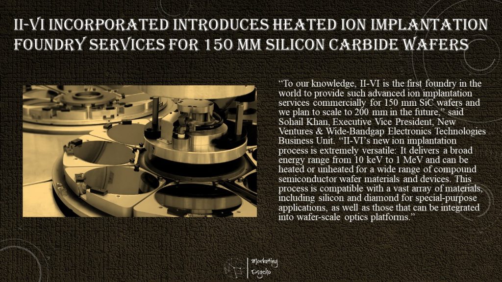
“To our knowledge, II‐VI is the first foundry in the world to provide such advanced ion implantation services commercially for 150 mm SiC wafers and we plan to scale to 200 mm in the future,” said Sohail Khan, Executive Vice President, New Ventures & Wide-Bandgap Electronics Technologies Business Unit. “II‐VI new ion implantation process is extremely versatile: It delivers a broad energy range from 10 keV to 1 MeV and can be heated or unheated for a wide range of compound semiconductor wafer materials and devices. This process is compatible with a vast array of materials, including silicon and diamond for special-purpose applications, as well as those that can be integrated into wafer-scale optics platforms.”
II‐VI implants tens of thousands of wafers per week and adds tools and capacity as required to support customers’ changing needs, provides capacity for urgent spikes in demand, and offers same-day turnaround. II-VI’s world-class technical expertise, rigorous quality program, and broad range of tooling offer a powerful and flexible outsourcing option for ion implantation, serving production manufacturing and R&D environments.
II‐VI maintains a large complement of high- and medium-current and high-energy production implanters handling 2-inch to 12-inch substrates. II‐VI broad range of wafer foundry services includes silicon carbide, gallium arsenide, and indium phosphide epitaxial growth. II‐VI also provides ion implantation disk refurbishing and reconditioning services to maximize quality, uptime, and utilization.
Toshiba’s New Device Structure Improves SiC MOSFET High Temperature Reliability and Reduces Power Loss
Toshiba Electronic Devices & Storage Corporation has developed a new SiC MOSFET device structure that simultaneously achieves higher reliability at high temperatures and lower power loss. In a 3300V chip at 175℃, a level of current over double that of Toshiba’s present structure, the new structure operates without any loss of reliability, and it also reduces specific on-resistance at room temperature by about 20% for a 3300V chip and 40% for a 1200V chip.
Silicon carbide (SiC) is widely seen as the next generation material for power devices, as it delivers higher voltages and lower losses than silicon. While SiC power devices are now mainly utilized in inverters for trains, wider application is on the horizon, including in photovoltaic power systems and the power management systems of industrial equipment. However, the use and market growth of SiC devices have been held back by reliability issues. One problem is the expansion of crystal defects when current flows through the PN diode positioned between a power MOSFET’s source and drain, which increases on-resistance and degrades device reliability.
Toshiba developed a novel device structure, a MOSFET with an embedded a Schottky barrier diode (SBD) that made progress in solving this problem. This was reported at PCIM Europe 2020, an international power semiconductor conference, and introduced into products in August 2020. That structure prevents PN diode operation by positioning an SBD in parallel to the PN diode in the MOSFET; the embedded SBD has a lower on-state voltage than the PN diode, and current flows through it, suppressing changes in on-resistance.
However, that structure can handle only limited current density at high temperatures of 175℃ or more. Accelerated adoption of SiC devices requires SiC devices that maintain high current capability and high reliability at high temperatures.
The new structure is a modification of the SBD-embedded MOSFET device, achieved by applying a 25% process shrink and optimizing the design to strengthen the SBD’s suppression of current in the PN diode. This has realized a 3300V chip structure with more than double the current density at 175℃ compared to Toshiba’s present structure without loss of reliability. The structure also reduces specific on-resistance by about 20% in a 3300V chip and about 40% in a 1200V chip at room temperature.
Details of the achievement were reported at PCIM Europe 2021, and the IEEE-sponsored International Symposium on Power Semiconductor Devices and ICs 2021 (ISPSD 2021), both held online.
Toshiba started sample shipment of a 3.3kV class SiC power module with the new structure in May this year.
BYD Semiconductor Bumps Prices by 5% as Global Chip Shortage Persists
The Chinese automaker’s chip division BYD Semiconductor is one of 30 semiconductor companies to raise prices this year.
BYD Semiconductor will raise the price of IPM (intelligent power module) and IGBT (insulated-gate bipolar transistor) products by at least 5% starting July 1, citing increased cost of inputs from upstream suppliers resulting from the global chip shortage. The company’s announcement was circulated via a letter to customers.
The worldwide shortage of integrated circuits that began in the second half of 2020 has extended into 2021. It has caused many producers to increase their prices. BYD was one of 30 semiconductor firms that have raised prices by 5–30% since the beginning of Q2 2021.
Even major foundries like UMC and TSMC have had to adjust their pricing strategy and said they will hike prices again in the third quarter by as much as 30%, according to local media reports. The rate is well beyond the industry’s expectations of a 15% lift.
As relentless demand is set to outpace global chip supply for the rest of 2021, per a report from Tianfeng Securities, foundries are upping their production capacity. Meanwhile, Chinese investors are pouring billions of yuan into new chip projects, with the aim of producing 8-inch and 12-inch wafers, which are used in products like mobile phone chips, camera sensors, wireless communication chips, and automobile chips.
In China, the construction or planning of at least 40 new 12-inch wafer fabs is currently underway. However, investors should be wary amid the frenzy to create semiconductor companies, as not all chip projects are qualified, resulting in some ill-advised ventures ending in failure.
Nagoya Institute of Technology and NGK Establish “NGK Environment Innovation Laboratory”
Nagoya Institute of Technology and NGK INSULATORS, LTD. both based in Nagoya, Japan, have established the NGK Environment Innovation Laboratory on the NITech campus. This collaboration between the private sector and academia will work on creating innovative next generation products that contribute to a significant reduction of greenhouse gases, such as materials for next-generation power semiconductors and high-performance storage batteries.
The NGK Environment Innovation Laboratory is headed by Professor Tomokatsu Hayakawa of the NITech with Project Professor Hideki Mori and NGK’s Shinji Kawasaki as deputy directors. Five NITech professors with different fields of expertise will initially engage in three research and development with NGK’s R&D division. The project will run for five years.
In its mid-to long-term vision NGK Group Vision: Road to 2050 formulated in April 2021, NGK identified carbon neutrality (net zero volume of greenhouse gas emissions) as one of its priority social issues. Since 2009, the NITech and NGK have engaged in a comprehensive collaboration program including joint research and technological exchange. The NGK Environment Innovation Laboratory was established as part of this collaboration under the NITech’s project laboratory program to focus on development related to carbon neutrality. The laboratory project will engage in research and development of next-generation power semiconductor wafers essential for energy-saving electronic devices and electric vehicles (EV), ceramic solid-state electrolytes and separators with high ionic conductivity for high-performance storage batteries that are indispensable to utilize renewable energy.
These research themes are included in the 39 themes identified in the Japanese Government Cabinet Office’s “Environment Innovation Strategy” set in 2020 and can take advantage of NGK’s ceramics technologies. The laboratory will consider taking on additional research themes that contribute to inventive environmental innovations and themes related to materials informatics going forward.
New Semiconductor Fabs to Spur Surge in Equipment Spending
Semiconductor manufacturers worldwide will have started construction on 19 new high-volume fabs by the end of this year and break ground on another 10 in 2022 to meet accelerating demand for chips across a wide range of markets including communications, computing, healthcare, online services and automotive, according to SEMI’s quarterly World Fab Forecast report. Equipment spending for the 29 fabs is expected to surpass $140 billion over the next few years.
China and Taiwan will lead the way in the new fab construction starts with eight each, followed by the Americas with six, Europe/Mideast with three, Japan and Korea with two each. Fabs that produce 300mm wafers will account for most of the new facilities – 15 – in 2021 and again in 2022, when seven fabs will begin construction. The remaining seven fabs planned over the two-year period will be 100mm, 150mm and 200mm facilities. The 29 fabs could produce as many as 2.6 million wafers per month (in 200mm equivalents).
Of the 29 fabs starting construction in 2021 and 2022, 15 are foundry facilities with capacities ranging from 30,000 to 220,000 wafers per month (200mm equivalents). The memory sector will begin construction on four fabs over the two-year span. Those facilities will boast higher capacities ranging from 100,000 to 400,000 wafers per month (200mm equivalents).
Of the semiconductor makers beginning construction of new fabs this year, many won’t start installing equipment until 2023 since it takes up to two years after ground is broken to reach that phase, though some could begin equipping as soon as the first half of next year.
While the World Fab Forecast shows 10 high-volume fabs starting construction next year, that number is likely to climb as chipmakers announce new facilities. The report tracks investments for fab construction and fab equipment, in addition to capacities, products and technologies from 2021 through 2022.
In addition to the 29 high-volume fabs, the World Fab Forecast report tracks 22 low-probability projects that could begin construction in 2021. Work on another 15 low-probability projects could start the following year.
EE Awards Asia
EE Awards Asia celebrates some of the best products, companies, and industry executives making a difference every day in Asia’s electronics industry. It honors the people and companies in Asia, which are behind the technologies that are changing the way we work, live, and play.
The 2021 EE Awards Asia winners are selected by a committee comprised of ASPENCORE’s global senior industry analysts, as well as online readers and users across Asia.
You can join EE Awards Asia in honoring these extraordinary achievements in the field of semiconductor industry this year. Voting ends on July 09, 2021.
Subscribe to Power Semiconductors Weekly and watch it on YouTube every Tuesday.
If you prefer a monthly update about the world of power semiconductors delivered to your e-mail address, please, subscribe to Marketing Psycho Power Semiconductors newsletter.