Power Semiconductors Weekly Vol. 94
Coherent Partners with ETRI and KAIST to Focus on Advanced Semiconductor Devices for the Korean Market
Coherent Corp., a global leader in materials, networking, and lasers, announced that it has signed a memorandum of understanding with two Korean institutions, the Electronics and Telecommunications Research Institute (ETRI) and the Korea Advanced Institute of Science & Technology (KAIST), to foster collaboration on advanced electronic and photonic devices, with a focus on the Korean market.
The MoU was signed in conjunction with the Korea-US Industrial Cooperation Forum, which provides a mutual collaboration platform for both countries with the support of the U.S. Department of Commerce; Korea’s Ministry of Trade, Industry, and Energy (MOTIE); and the Korea Institute for Advanced Technology (KIAT).
Korea is at the forefront of new technologies that are transforming industries such as communications, automotive, and consumer electronics. Coherent technology platforms are ideally suited to enable a broad range of existing and emerging applications in these rapidly growing markets.
“Korea continues to be a strategic market for Coherent, and we really look forward to expanding our relationship with such well-respected partners as ETRI and KAIST,” said Dr. Julie Sheridan Eng, Chief Technology Officer, Coherent Corp. “We will begin by reviewing our respective technology roadmaps and identifying areas of synergistic interest where we can advance the state of the art and accelerate technology development in Korea.”
The partnership announced will cover a broad range of innovations in devices, leveraging silicon carbide, gallium arsenide, and indium phosphide technology platforms. The collaboration will address applications in power electronics for electric vehicles, industrial applications, and optical and wireless networks.
LA Semiconductor Purchases Fabrication Plant From onsemi
LA Semiconductor, the newest U.S. owned and operated pure-play semiconductor foundry for analog, mixed signal and power products, announced the purchase of the Pocatello, Idaho fabrication plant from onsemi.
“onsemi’s trust in LA Semiconductor as a key supplier, new owner and operator of the Pocatello fab is a testament to the deep experience and potential that our team brings to the marketplace,” said Mike Ward, Founder, President and CEO of LA Semiconductor. “There is an ongoing need for more chip manufacturing capacity in this country, both for mature market segments, such as discrete and power devices, and for tomorrow’s advanced products and technologies. With the U.S. government fully aligned on supporting our industry through the passage of The CHIPS and Science Act of 2022, we are optimistic about what the future holds.”
LA Semiconductor is a spin-off of Linear ASICs Inc., a turn-key ASIC design services company with expertise in analog, power and mixed-signal semiconductors. Linear ASICs will continue providing design services to some of LA Semiconductor’s customers and will bring foundry manufacturing opportunities to LA Semiconductor.
Macquarie Group provided financing to facilitate the purchase of the Idaho fabrication plant and the subsequent launch of LA Semiconductor.
“With so few foundries in the US and the government alignment for onshore solutions, we saw this as an ideal time to invest in LA Semiconductor’s mission to deliver a high-quality, steady supply of chips to the U.S. market,” said Don Trent, Managing Director in Macquarie’s Semiconductor & Technology business within the Commodities and Global Markets group.
“This investment will not only support LA Semiconductor on a go-forward basis, but it is a reflection of our commitment to support semiconductor growth across the spectrum from mature to leading edge technology nodes. We have the experience and expertise in semiconductor production equipment to both understand the assets and the marketplace. We’re proud to be supporting LA Semiconductor to advance its capacity, capabilities and technology to serve new and existing customers.”
Toshiba to Expand Power Semiconductor Production Capacity with New Production Facility
Toshiba Electronic Devices & Storage Corporation (“Toshiba”) announced that it will construct a new back-end production facility for power semiconductors at its Himeji Operations – Semiconductor, in Hyogo Prefecture in western Japan. Construction will start in June 2024, with production scheduled to start in spring 2025. The project will more than double Toshiba’s automotive power semiconductor production capacity at Himeji, against fiscal 2022.
Power devices are essential components for managing and reducing power consumption in all kinds of electronic equipment, and for saving energy. Above all other products, demand for low-voltage MOSFETs (metal oxide semiconductor field effect transistors), a Toshiba focus technology, is expected to see continued growth with the progress of vehicle electrification and the automation of industrial equipment. Toshiba has decided to meet this demand growth with construction of the new back-end facility.
Going forward, Toshiba will expand its power semiconductor business and boost competitiveness by offering high efficiency, high reliability products in response to fast growing demand, and to contribute to carbon neutrality.
Hunan Sanan Secures Order for $524 Million from a Leading NEV Brand
Sanan Optoelectronics, a publicly traded company, issued an announcement that Hunan Sanan, its subsidiary, signed a procurement letter of intent (LOI) agreement with a strategic automotive partner. According to the agreement, Hunan Sanan will supply silicon carbide (“SiC”) chips to the automaker’s new electric vehicle (“NEV”) product line in the next few years, totaling $524 million USD.
Tony Chiang, General Manager of Hunan Sanan, said, “Our agreement with this strategic partner further demonstrates the automotive industry’s commitment to providing innovative electrification experience to the market and leveraging the advantages of wide bandgap semiconductors to improve overall vehicle performance. The agreement ensures a long-term supply of SiC to our customer to help them realize their promise of low-carbon, smart mobility.”
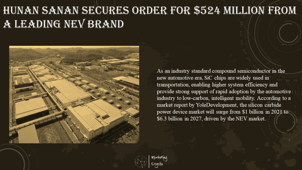
The SiC chips in the agreement will be manufactured in the Hunan Sanan’s mega fab in Changsha, the first vertically integrated SiC wafer manufacturing service platform in China, providing in-house supply chain from SiC crystal, substrate, epitaxy, chip manufacturing, packaging and testing, with a committed annual production capacity of 500,000 silicon carbide 6-inch wafers.
Hunan Sanan has recently obtained IATF 16949 system certification while the automotive-grade SiC MOSFETs have been verified with the cooperation of strategic partners, and are expected to be released in production in 2024. Sike Semiconductor, a company jointly established by Hunan Sanan and Li Auto, also officially started construction this past August and is expected to start production in 2024 with a planned annual production capacity of 2.4 million half-bridge SiC power modules.
As an industry standard compound semiconductor in the new automotive era, SiC chips are widely used in transportation, enabling higher system efficiency and provide strong support of rapid adoption by the automotive industry to low-carbon, intelligent mobility. According to a market report by YoleDevelopment, the silicon carbide power device market will surge from $1 billion in 2021 to $6.3 billion in 2027, driven by the NEV market. However, due to the gap between the high demand of NEV’s and the expansion of SiC substrate manufacturing, the supply of silicon carbide chips will be in a shortage in the short term. Automakers have started partnering with strategic upstream suppliers for their chips to ensure that NEV manufacturing can continue to secure critical components.
Hunan Sanan’s SiC technology will provide energy for the NEV power system for medium and high voltage platforms, and will empower the high voltage analog IC supply chain to create a low-carbon intelligent vehicle experience and help achieve a green energy lifestyle.
Applied Materials to Extend Global Leadership in Semiconductor Manufacturing Technology
Applied Materials, Inc. announced its intention to make multi-billion-dollar investments in its innovation infrastructure in the United States and to expand its global manufacturing capacity between now and 2030. These investments will enhance customer collaboration to accelerate improvements in semiconductor performance, power and cost – and enable the company to increase equipment manufacturing capacity as the digital transformation of the economy creates the opportunity for a $1 trillion semiconductor market.
“Applied Materials is the world leader in materials engineering solutions – the foundational technologies that define how current and future generations of chips are made,” said Gary Dickerson, President and CEO. “With these investments, we will double our innovation infrastructure in the United States and significantly expand our ability to serve customers building new fabs in America and around the world.”
At the heart of these investments, the scale of which will be contingent upon receiving government support, Applied Materials plans to build a next-generation R&D center in Sunnyvale, California. This high-velocity innovation platform will be dedicated to advancing materials engineering, foundational semiconductor technologies and process equipment. The Silicon Valley center will play a central role in collaborative research and development with all the world’s major chipmakers, bolster university partnerships, and be capable of engaging with a future U.S. National Semiconductor Technology Center. Applied expects to make this investment with support from the U.S. government through provisions of the CHIPS and Science Act and the State of California through the Governor’s Office of Business and Economic Development (GO-Biz) California Competes Grant awarded earlier this year. An event to mark the launch of this investment is planned for early 2023 in Silicon Valley.
In addition, Applied Materials intends to expand its U.S. equipment manufacturing capacity as well as invest in new infrastructure to both accelerate collaboration with the industry ecosystem and develop the talented workforce needed to build America’s strength in critical future technologies. The investment in manufacturing capacity will expand the company’s factories in Austin, Texas which has been the home of Applied’s volume-manufacturing operations since 1993.
“Applied Materials has deep core capabilities in the U.S. – from our research centers in California and New York, to our factories in Texas and our product operations in Massachusetts and Montana,” said Dickerson. “No other semiconductor equipment company has a comparable footprint in the U.S., and we intend to invest boldly and build on this world-class infrastructure to accelerate our technology leadership and enable our customers’ growth for decades to come.”
Applied is also investing in its global infrastructure and will hold a groundbreaking ceremony for an expansion of its regional hub in Singapore on December 22, which, together with the planned expansion in the U.S., will significantly increase Applied Materials’ capacity to serve growing worldwide demand for semiconductors.
Supervisory Board Appoints Dr. Michael Heckmeier as Future CEO Of Siltronic AG
The Supervisory Board of Siltronic AG has appointed Dr. Michael Heckmeier as future CEO. He succeeds Dr. Christoph von Plotho, who has led the Company as CEO since 2010 and who will retire. Michael Heckmeier will take up his position on July 1, 2023 at the latest and has been appointed for an initial period of three years.
We are very pleased to introduce Dr. Michael Heckmeier as an experienced successor to Dr. Christoph von Plotho,” said Dr. Tobias Ohler, Chairman of the Supervisory Board of Siltronic AG. “Michael Heckmeier holds a doctorate in physics. He worked for Merck KGaA for almost 25 years. After holding positions in R&D, Innovation, New Ventures in Germany and England, he has been heading the Display Solutions business as Executive Vice President since 2017. He is highly experienced internationally and knows the Asian markets very well. As CEO Michael Heckmeier will lead Siltronic AG into the future with continued great success.“
„We would like to thank Christoph von Plotho sincerely for his outstanding work at the top of Siltronic. Over the past 12 years, Christoph von Plotho has played a key role in shaping Siltronic’s success story and will leave a strong foundation for future generations. Under his leadership, Siltronic was successfully listed on the stock exchange in 2015, the Company’s operating performance and profitability were significantly improved and Siltronic was developed into one of the technology leaders in the wafer market. Additionally, in 2021, it was decided to build a new fab in Singapore. The Company owes a great deal to Christoph von Plotho, whose achievements deserve our highest respect and recognition.“
Subscribe to Power Semiconductors Weekly and watch it on YouTube every Tuesday.
If you prefer a monthly update about the world of power semiconductors delivered to your e-mail address, please, subscribe to Marketing Psycho Power Semiconductors newsletter.