Power Semiconductors Weekly Vol. 85
Next Generation Uninterruptible Power Supplies with SiC Solutions from Leapers Semiconductor
Digitalization, growth of cloud technologies, AI, ongoing pandemic, decarbonization plans, and the other global trends set new standards, requirements, and challenges to power electronics industry, especially to end products like uninterruptible power supplies (UPS).
An uninterruptible power supply is an electrical system that provides emergency power to a load when the input power source or mains power fails. A UPS differs from an auxiliary or emergency power system or standby generator in that it will provide near-instantaneous protection from input power interruptions, by supplying energy stored in batteries, supercapacitors, or flywheels. The on-battery run-time of most uninterruptible power sources is only a few minutes but sufficient to start a standby power source or properly shut down the protected equipment. It is a type of continual power system.
Uninterruptible power supplies are typically used to protect computers, data centers, telecommunication equipment or other electrical equipment where an unexpected power disruption could cause injuries, fatalities, serious business disruption or data loss.
There are four main components in an uninterruptible power supply system: rectifier, batteries, inverter, and static bypass switch.
Power semiconductors industry has always been the major drive force for power electronics. And with introduction of silicon carbide (SiC) as the successor of silicon (Si) it became possible for engineers to provide more compact, power efficient, highly reliable solutions using the new generation power modules. This rule also applies to UPS.
For a long time, power semiconductors like thyristors, diodes, and IGBTs were used for rectifiers and inverters of the UPS. However, with the mass introduction of SiC devices it became possible to design more compact and efficient UPS systems.

Nowadays more manufacturers of uninterruptible power supplies are searching for the ways to deliver new generation systems with new generation power semiconductors. And many of them tend to choose SiC power modules instead of IGBTs for their new designs.
Leapers Semiconductor’s wide SiC power modules portfolio includes top solutions for the UPS industry. Thus, E2 series SiC power modules correspond to all requirements of UPS R&D engineers. All E2 series SiC power modules provide best in class low switching losses.
Among other features of E2 modules are:
- 1200 V blocking voltage
- Rdson 4,5-20 mOhm
- Si3N4 DBC
- Thermistor inside
- 175°C maximum junction temperature
- Low thermal resistance
- High insulation and voltage resistance
- CTI > 400
- High-speed switching
In order to facilitate customers’ requirements to test and simulate the performance of the SiC MOSFET modules, Leapers Semiconductor has developed demo driver board designed specifically for E2 series.
At the moment Leapers Semiconductor offers 1200 V E2 series SiC power modules in Half-Bridge and H-Bridge topologies with Rdson varying from 4,5 to 20 mOhm:
- DFS04HF12EZR1 / Half-Bridge / 4.5 mOhm
- DFS05HF12EZR1 / Half-Bridge / 5.5 mOhm
- DFS09HF12EZR1 / Half-Bridge / 9 mOhm
- DFS09HH12EZR1 / H-Bridge / 9 mOhm
- DFS20HH12EZQ1 / H-Bridge / 20 mOhm
Leapers Semiconductor innovative approach to product development results in high performance products. E2 series is no exception. Now all customers can benefit from these SiC MOSFET modules to design more efficient and compact product which will not only save time and money for end customers, but deliver long time excellent performance with no additional maintenance system cost.
Renesas Unveils New-Generation Si IGBTs for Electric Vehicle Inverters
Renesas Electronics Corporation announced the development of a new generation of Si-IGBTs (Silicon Insulated Gate Bipolar Transistors) which will be offered in a small footprint while providing low power losses. Aimed at next generation electric vehicle (EVs) inverters, AE5-generation IGBTs will be mass produced starting in the first half of 2023 on Renesas’ 200- and 300-mm wafer lines at the company’s factory in Naka, Japan. Additionally, Renesas will ramp up production starting in the first half of 2024 at its new power semiconductor 300-mm wafer fab in Kofu, Japan to meet the growing demand for power semiconductor products.
The silicon based AE5 process for IGBTs achieve a 10% reduction in power losses compared to the current-generation AE4 products, a power savings that will help EV developers save battery power and increase driving range. In addition, the new products are approximately 10% smaller while maintaining high robustness. The new Renesas devices achieve the industry’s highest level of performance for IGBTs by optimally balancing low power loss and robustness tradeoffs. Moreover, the new IGBTs significantly improve performance and safety as modules by minimizing parameter variations among the IGBTs and providing stability when operating IGBTs in parallel. These features provide engineers greater flexibility to design smaller inverters that achieve high performance.
“Demand for automotive power semiconductors is rapidly growing, as EVs become more widely available,” said Katsuya Konishi, Vice President of Renesas’ Power System Business Division. “Renesas’ IGBTs provide highly reliable, robust power solutions that build on our experience in manufacturing automotive-grade power products for the last seven years. With the latest devices soon to be in mass production, we are providing optimal features and cost performance for mid-range EV inverters that are expected to grow rapidly in the future.”
Key Features of the New-Generation IGBT (AE5)
- Four products targeting 400-800V inverters: 750V withstand voltage (220A and 300A) and 1200V withstand voltage (150A and 200A)
- Steady performance throughout the operating junction temperature (Tj) range from -40°C to 175°C
- Industry’s highest performance level with an on-voltage Vce (saturation voltage) of 1.3V, a key value for minimizing power loss
- 10% higher current density compared to conventional products and small chip size (100mm2/300A) optimized for low power losses and high input resistance
- Stable parallel operation by reducing parameter variations to VGE(off) to ±0.5V
- Maintains reverse bias safe operating area (RBSOA) with a maximum Ic current pulse of 600A at 175°C junction temperatures, and a highly robust short circuit withstand time of 4µs at 400V.
- 50% reduction in the temperature dependence of gate resistance (Rg). This minimizes switching losses at high temperatures, spike voltage at low temperatures and short circuit withstand time, supporting high performance designs.
- Available as a bare die (wafer)
- Enables a reduction in inverter power losses, improving power efficiency by up to 6% compared to the current AE4 process at the same current density, allowing EVs to drive longer distances and use fewer batteries.
In EVs, the motors that power vehicles are controlled by inverters. Switching devices such as IGBTs are critical in minimizing power consumption for EVs, as inverters convert DC power to the AC power that electric vehicle motors require. To assist developers, Renesas offers the xEV Inverter Reference Solution, a working hardware reference design that combines an IGBT, microcontroller, power management IC (PMIC), gate driver IC, and fast recovery diode (FRD).
Renesas also offers the xEV Inverter Kit, which is a hardware implementation of the reference design. In addition, Renesas provides a motor parameter calibration tool and the xEV Inverter Application Model and Software, which combines an application model and sample software for controlling the motor. These tools and support programs from Renesas are designed to help customers simplify their software development efforts. Renesas plans to add the new-generation IGBTs to these hardware and software development kits to enable even better power efficiency and performance in a smaller footprint.
Toshiba Launches Third Generation 650V SiC MOSFETs
Toshiba Electronics Europe GmbH (“Toshiba”) has launched a total of five new third-generation 650V silicon carbide (SiC) MOSFET devices for industrial equipment.
These highly efficient and versatile products will be used in a variety of demanding applications including switch mode power supplies (SMPS) and uninterruptible power supplies (UPSs) for servers, data centers and communication equipment. They will also find applications in renewable energy, including photovoltaic (PV) inverters and bi-directional DC-DC converters, such as those used for electric vehicle (EV) charging.
The new TW015N65C, TW027N65C, TW048N65C, TW083N65C and TW107N65C are based upon Toshiba’s advanced third generation SiC process which optimizes the cell structures used in second-generation devices.
As a result of this advancement, a key figure of merit (FoM) calculated as the product of drain-source on-resistance (RDS (on)) and gate-drain charge (Qg) to represent both static and dynamic losses have improved by about 80%. This significantly reduces losses and allows power solutions with higher power densities and lower running costs to be developed.
In common with earlier devices, the new third-generation MOSFETs include a built-in SiC Schottky barrier with a low forward voltage (VF) of -1.35V (typ.) to suppress fluctuation in RDS(on), thereby enhancing reliability.
The new devices are able to handle currents (ID) up to 100A and feature RDS(on) values as low as 15mΩ. All devices are housed in an industry standard TO-247 package.
SK Siltron CSS Opens a New Fab in Gumi
SK Siltron CSS CEO Jianwei Dong, Ph.D. and other executive leaders recently had the honor of joining the SK Siltron team in Gumi, South Korea, to celebrate the commissioning of their state-of-the-art SiC fab facility. Not only will this facility increase SiC wafering and epitaxy capacity, but it will also strengthen capability in the high-volume manufacturing of semiconductor wafers.
Collaborative efforts are truly what it took the Gumi and CSS team to build and commission the fab in record time. In tandem with the Bay City fab, soon to have its own ribbon-cutting celebration, the Gumi fab will enable SK Siltron CSS to keep up with the constantly-rising SiC demand.
Marelli Motorsport and Politecnico di Torino Cooperate on GaN
Marelli Motorsport – the Motorsport business unit of the global automotive supplier Marelli, with an extensive experience in the development of hybrid and electric systems for major motorsport championships – and the Power Electronics Innovation Center (PEIC) of Politecnico di Torino announced a new collaboration, regarding the Gallium Nitride (GaN) technology area for power electronics, aimed at electric engines. The project is included in a wider framework research partnership between Marelli and Politecnico.
The collaboration is aiming at the design and prototyping of an innovative multi-level 900V high power inverter for electric traction based on GaN technology.
Gallium Nitride, a cutting-edge technology reaching unprecedented switching frequencies and low switching energy, allows a radical reduction of passive components (e.g. inductors, capacitors, transformers), while maintaining an outstanding efficiency. In the last years, the GaN technology has been evolving rapidly in terms of conduction and switching performance. In addition, since the lateral GaN devices are grown on standard silicon wafers, their cost is already highly competitive.
GaN technology opens new horizons in the power converter design innovations, in which the collaboration has the aim to excel in terms of high efficiency multilevel architectures, optimal and robust gate driving and device parallelization, high frequency and high temperature capacitor technologies, integration of capacitors and semiconductors on PCB (Printed Circuit Board) for cost reduction, advanced cooling solutions.
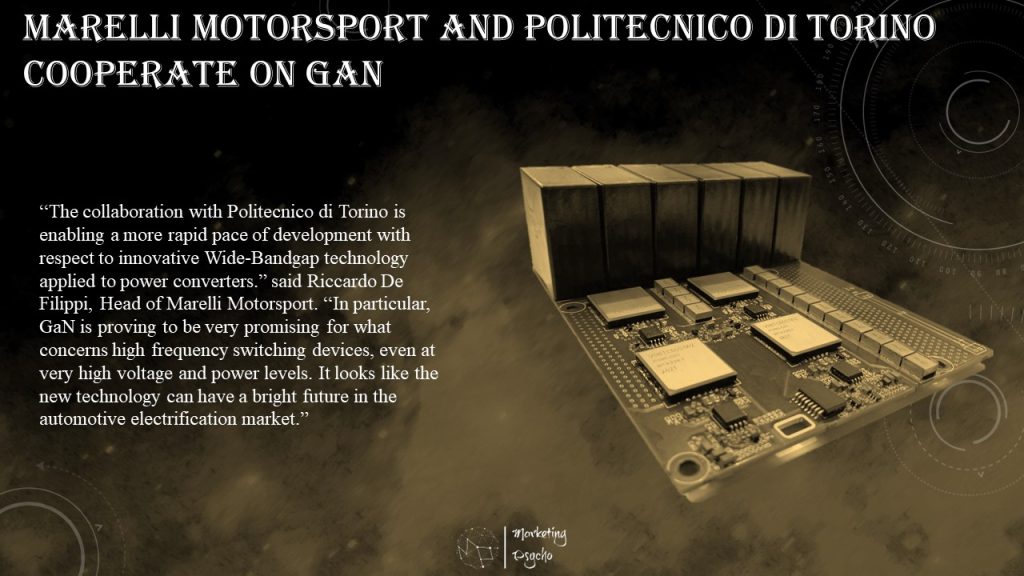
“The collaboration with Politecnico di Torino is enabling a more rapid pace of development with respect to innovative Wide-Bandgap technology applied to power converters.” said Riccardo De Filippi, Head of Marelli Motorsport. “In particular, GaN is proving to be very promising for what concerns high frequency switching devices, even at very high voltage and power levels. It looks like the new technology can have a bright future in the automotive electrification market.”
Radu Bojoi, Politecnico di Torino, chairman of Power Electronics Innovation Center (PEIC), commented: “The collaboration with Marelli is a further demonstration of the multiple benefits and synergies possible between University and Industry when they join forces in fast tracking new technologies into cutting edge device development.”
The concept study started back in 2021 and at present it is in the prototyping phase, which is planning to undergo two development steps withing 2022. The GaN component supplier selected for the prototype phase is VisIC Technologies, a global leader in gallium nitride (GaN) solutions for high-voltage automotive applications.
“The project with Marelli and PEIC for the development of gallium nitride-based multi-level-power inverters in electric vehicles illustrates the break-through of gallium nitride technology in the automotive industry,” said Tamara Baksht, CEO of VisIC. “VisIC’s D3GaN technology was developed for the high reliability standards of the automotive industry and offers the lowest losses per RDS(on). It also simplifies the system solution and enables high-efficiency and affordable power train solutions. It is definitely the next step for the automotive electrical driveline.”
Beyond the motorsport domain, which is always at the forefront of innovation thanks to its capability to design and test technologies in a fast way and challenging conditions, the know-how and technologies developed in the frame of this collaboration, for Marelli will be crucial also to enable a technological flow-down to series production technologies.
Wolfspeed Webinar: Build More Efficient Solar Inverters and Energy Storage Systems with SiC
Silicon Carbide MOSFETs and Schottky Diodes are revolutionizing the solar photovoltaic (PV) industry, enabling increased switching speeds and energy efficiency, resulting in smaller, lighter, lower-cost systems.
Join Wolfspeed for this webinar where you will explore the fast-growing lower power 5-15 kW single and three phase PV energy storage system (ESS) where new Silicon Carbide device and package options are enabling cost/performance optimized solutions for residential and smaller commercial applications.
Key Take-Aways:
- Energy storage is driving renewed growth in the PV industry
- MPPT boost, inverter and battery charging circuits benefit significantly from Silicon Carbide devices
- Date: September 19, 2022
- Time: 5 PM CEST
Subscribe to Power Semiconductors Weekly and watch it on YouTube every Tuesday.
If you prefer a monthly update about the world of power semiconductors delivered to your e-mail address, please, subscribe to Marketing Psycho Power Semiconductors newsletter.