Power Semiconductors Weekly Vol. 79
Bosch Invests Further Billions in Chip Business
From cars and e-bikes to household appliances and wearables – semiconductors are an integral part of all electronic systems. They are the motor that drives the modern world of technology. Bosch recognized their growing significance early on and has now announced investment of further billions of euros in order to strengthen its own semiconductor business. By 2026, Bosch plans to invest another 3 billion euros in its semiconductor division as part of the IPCEI funding program on microelectronics and communications technology. “Microelectronics is the future and is vital to the success of all areas of Bosch business. With it, we hold a master key to tomorrow’s mobility, the internet of things, and to what we at Bosch call technology that is ‘Invented for life’,” says Dr. Stefan Hartung, chairman of the Bosch board of management, at the Bosch Tech Day 2022 in Dresden.
One of the projects Bosch plans to fund with this investment is the construction of two new development centers – in Reutlingen and Dresden – at a combined cost of over 170 million euros. In addition, the company will spend 250 million euros over the coming year on the creation of an extra 3,000 square meters of clean-room space at its wafer fab in Dresden. “We’re gearing up for continued growth in demand for semiconductors – also for the benefit of our customers,” Hartung said. “For us, these miniature components mean big business.”
Within the framework of the European Chips Act, the European Union and German federal government are providing additional funding to develop a robust ecosystem for the European microelectronics industry. The objective is to double Europe’s slice of global semiconductor production from 10 to 20 percent by the end of the decade. The newly launched IPCEI on Microelectronics and Communication Technology is intended primarily to promote research and innovation. “Europe can and must capitalize on its own strengths in the semiconductor industry,” Hartung said. “More than ever, the goal must be to produce chips for the specific needs of European industry. And that means not only chips at the bottom end of the nanoscale.” Electronic components used in the electromobility industry, for example, require process sizes of between 40 and 200 nanometers. This is exactly what the Bosch wafer fabs are designed for.
This new investment in microelectronics also opens up new areas of innovation for Bosch. “Being a leader in innovation begins with the very smallest of electronic components: semiconductor chips,” Hartung said. New fields of innovation at Bosch include systems-on-a-chip, such as the radar sensors a vehicle uses to perform 360-degree scans of its surroundings during automated driving. Bosch will now be looking to enhance such components, making them smaller, smarter, and also cheaper to produce. The company is also working to further modify its own microelectromechanical systems (MEMS) specifically for the consumer goods industry. One of the things company researchers are currently using this technology to develop is a new projection module that is so tiny it can be built into the temple of a pair of smart glasses. “In order to cement our leading market position in MEMS technology, we also plan to manufacture our MEMS sensors on 300-millimeter wafers,” Hartung said. “Production is scheduled to start in 2026. Our new wafer fab gives us the opportunity to scale production – an advantage we intend to exploit to the full.”
A further focal point at Bosch is the production of new types of semiconductors. At its Reutlingen plant, for example, Bosch has been mass-producing silicon carbide (SiC) chips since the end of 2021. These are used in the power electronics required for electric and hybrid vehicles, where they have already helped boost operating ranges by up to 6 percent. On the back of powerful market growth, at annual rates of 30 percent or more, demand for SiC chips remains high, meaning full order books for Bosch. In a bid to make these power electronics more affordable and more efficient, Bosch is exploring the use of other types of chips as well. “We’re also looking into the development of chips based on gallium nitride for electromobility applications,” Hartung said. “These chips are already found in laptop and smartphone chargers.” Before they can be used in vehicles, they will have to become more robust and able to withstand substantially higher voltages of up to 1,200 volts. “Challenges like these are all part of the job for Bosch engineers. Our strength is that we’ve been familiar with microelectronics for a long time – and we know our way around cars just as well.”
Bosch has made several investments in its semiconductor business over the past few years. The best example of this is the wafer fab in Dresden, which opened in June 2021. At 1 billion euros, it is the single biggest investment in the company’s history. The semiconductor center in Reutlingen is also being systematically expanded: between now and 2025, Bosch is to invest around 400 million euros in the expansion of manufacturing capacity and the conversion of existing factory space into new clean-room space. This includes construction of a new extension in Reutlingen, which will create an additional 3,600 square meters of ultramodern clean-room space. All in all, clean-room space in Reutlingen is set to grow from around 35,000 square meters at present to over 44,000 square meters by the end of 2025.
Bosch is the automotive industry’s leading company for the development and manufacture of semiconductors. These chips are used not only in automotive applications but also in the consumer goods industry. Bosch has been active in this field for over 60 years. The Bosch semiconductor plant in Reutlingen, for example, has been producing chips based on 150- and 200-millimeter wafers for the past 50 years. At the company’s Dresden plant, manufacture of chips on the basis of 300-millimeter wafers commenced in 2021. Among the semiconductors manufactured in Reutlingen and Dresden are application-specific integrated circuits (ASICs), microelectromechanical systems (MEMS) sensors, and power semiconductors. Bosch is also building a new test center for semiconductors in Penang, Malaysia. As of 2023, this center will be used to test finished semiconductor chips and sensors.
onsemi to Invest $1 Billion in Gyeonggi Research Center
U.S. chipmaker onsemi agreed to invest 1.4 trillion won ($1 billion) into building a new research center and manufacturing facility in Bucheon, Gyeonggi, to produce power chips by 2025.
The Gyeonggi provincial government announced that it signed a memorandum of understanding with the Phoenix, Arizona-based onsemi and held a ceremony to celebrate the commencement of construction of the manufacturing facility.
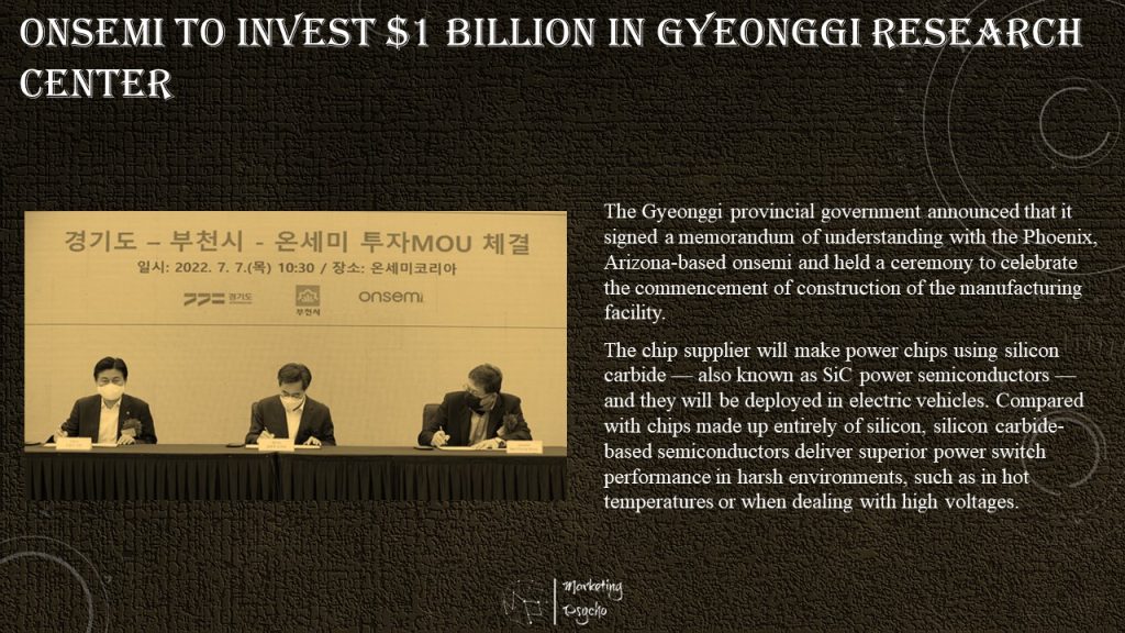
The chip supplier will make power chips using silicon carbide — also known as SiC power semiconductors — and they will be deployed in electric vehicles. Compared with chips made up entirely of silicon, silicon carbide-based semiconductors deliver superior power switch performance in harsh environments, such as in hot temperatures or when dealing with high voltages.
The new site could create 500 jobs. Alongside with the plan, onsemi will purchase 350-billion-won worth of raw materials, equipment and components from local suppliers.
Silicon Carbide Cooperation between SEMIKRON and ROHM Semiconductor
SEMIKRON, headquartered in Nuremberg, and the Kyoto-based company ROHM Semiconductor have been collaborating for more than ten years with regards to the implementation of silicon carbide (SiC) inside power modules. Recently, ROHM’s latest 4th generation of SiC MOSFETs has been fully qualified in SEMIKRON’s eMPack® modules for automotive use. Hence, both companies serve worldwide customers’ needs.
SEMIKRON announced it had secured a billion-Euro contract to supply their innovative eMPack® power modules to a major German car maker, beginning in 2025. The company developed a fully sintered assembly and connection technology ‘Direct Pressed Die’ (DPD). This enables extremely compact, scalable and reliable traction inverters. The eMPack® module technology has been specially designed for SiC-based converters of medium and high power in order to fully exploit the properties of the new semiconductor material. In addition, SEMIKRON provides evaluation boards for eMPack® that incorporate ROHM’s gate driver ICs, helping customers shorten the time required for evaluation and adoption. In the future, SEMIKRON also plans to use ROHM’s IGBTs in modules for industrial applications.
“Thanks to ROHM’s SiC technology, SEMIKRON’s innovative eMPack®- family of power modules is ready to make a significant contribution to reducing emissions through e-mobility,” says Karl-Heinz Gaubatz, CEO and CTO at SEMIKRON. “ROHM’s SiC technology provides more efficiency, performance and reliability in automotive and also industrial applications.”
ROHM produces SiC components in-house in a vertically integrated manufacturing system and thus delivers high quality, energy-saving products while achieving a constant market supply. ROHM’s production subsidiary SiCrystal, located in Nuremberg, Germany, plans to strongly grow its silicon carbide wafer capacities and human resources – to produce several 100,000 substrates a year.
“We are glad that SEMIKRON has selected ROHM as SiC supplier for the automotive qualified eMPack®. This partnership leads to a competitive solution for inverter application use inside electrical vehicles,” states Isao Matsumoto, President and CEO of ROHM Co., Ltd.. “ROHM offers a broad portfolio of SiC devices – from chips to packages. As the demand for SiC will continue to grow, ROHM will accelerate further investment and product development based on the technology we have cultivated as a leading SiC manufacturer. In addition, our company will continue to propose solutions and deliver customer support,” Isao Matsumoto continues.
ROHM has been a leader in SiC device technology and products since it began the world’s first mass production of SiC MOSFETs. ROHM’s latest 4th generation of SiC MOSFETs, which has been adopted by SEMIKRON, provides industry-leading low ON resistance with improved short-circuit withstand time. These characteristics contribute significantly to extend the driving length and miniaturize the batteries of EVs when they are used in traction inverters. Thus, the company develops advanced, energy-saving SiC devices that reduce environmental impact.
Both companies will continue to contribute to automotive technology innovations by providing optimal power solutions that meet market needs through the fusion of ROHM’s device/control technologies and SEMIKRON’s module technologies that can optimally combine them.
Soitec Boosts Customer Yield of SiC Manufacturing with KLA Inspection Technology
Soitec (Euronext Paris), an industry leader in designing and manufacturing innovative semiconductor materials, has selected KLA Corporation, a leader in process control and advanced inspection systems, to enable high yield manufacturing of innovative Silicon Carbide (SiC) devices for the automotive industry.
Soitec leverages its unique and patented SmartSiC™ technology to produce SiC substrates, which aim to improve the performance of power electronics devices and boost electric vehicles’ energy efficiency.
Based on its track record of using KLA’s inspectors for its Silicon-on-Insulator (SOI) wafers, Soitec has extended its partnership with KLA and selected the Surfscan® SP A2 unpatterned inspection system for its SmartSiC wafers.

Soitec’s SmartSiC wafers provide superior and unique crystal quality, while KLA’s Surfscan® SP A2 leverages DUV optics and advanced algorithms to support substrate quality control. This partnership will enable SiC substrate production at new and even more sophisticated levels, supporting the industry to bring high quality SiC semiconductors in high volumes to the automotive market.
In March 2022, Soitec announced the construction of a new fab, Bernin 4, at its headquarters in Bernin near Grenoble, France, primarily dedicated to the manufacturing of SmartSiC wafers in 150mm and 200mm size. The new fab is expected to be operational by the second half of 2023.
“Coupling our unique SmartSiC engineered substrates with KLA’s inspection and metrology systems will help us to assure supreme quality levels in the manufacturing of substrates and thus drive customer yield downstream,” said Christophe Maleville, Chief Technology Officer of Soitec. “With KLA, we have demonstrated the great potential of their inspection system for our all-important SOI technology. We now apply it to our innovative SmartSiC technology for the automotive sector. This will help us to drive our manufacturing efficiency, satisfy the growing demand from the electric vehicle market, and offer further added value to our customers.”
“At KLA we strongly value our customer relationships and R&D investment as they provide us with the knowledge and technologies needed to deliver the required process control solutions at the right time,” stated Jijen Vazhaeparambil, senior vice president of the Surfscan, ADE and ECI group. “Through our close collaboration with Soitec, we were able to adapt our world-class Surfscan inspection technology for the wide band gap substrate segment. The resulting Surfscan® SP A2 system provides the sensitivity and production capability needed to help Soitec achieve their stringent quality standards for SiC and other wide band gap substrates.”
IMEC to Help Set Up Semiconductor Units in India
Belgium-based semiconductor research organization IMEC (Interuniversity MicroElectronics Centre) has agreed to provide technical support to create a semiconductor ecosystem in India.
According to officials from the Ministry of Electronics and Information Technology (Meity), IMEC, which is known as an intermediate research organization in the world of semiconductor fabs, will also develop talent and research abilities in the country.
Last year in December 2021, the government approved a Rs 76,000-crore-PLI-scheme to boost semiconductor and display manufacturing in the country. The aim of the government is to make India a global hub for hi-tech production and attract large chipmakers around the world. So far, according to Meity minister Ashwani Vaishnaw, the scheme had received five applications for semiconductor and Display Fabs with total investment to the tune of $20.5 billion (Rs 153,750 crore).
Three companies including Vedanta in JV with Foxconn, IGSS ventures pte, Singapore and ISMC have submitted applications for semiconductor fabs. The official also said nearly 65% of semiconductors are used in electric vehicles, power, and telecom equipment and these industries demand big and mid-sized nodes. Therefore, there is a huge market for bigger process nodes and a significant market for mid-sized nodes.
Meanwhile, global electronics contract manufacturer Foxconn’s met Prime Minister Narendra Modi to expand its India’s operation. The Taiwan-based firm had signed a memorandum of understanding with Vedanta Group in February to form a joint venture company to set up an electronic chip manufacturing plant in India.
Talk to the Experts at Bodo’s Wide Bandgap Talk
Talk to the experts at Bodo’s wide bandgap talk! Join his virtual roundtable, focused on wide bandgap technology. This virtual open discussion goal is to keep the dialog going on, independent of any events that are hosted on fixed dates.
These expert talks are built on the articles Bodo published in his magazine, giving everyone the chance to ask questions to the experts out of the industry.

The next event is scheduled for tomorrow July 27. Find more information and register for the expert talk at Bodo’s Power Systems magazine website.
- Bodo’s wide bandgap talk next session will take place on July 27th
- SiC discussion from 3:00 to 4:00 pm CEST and GaN from 4:30 to 5:30 pm
- Platform of choice is ZOOM
PSMA PTR Webinar: SiC Power Technology Status and Barriers to Overcome
Silicon power devices have dominated power electronics due to their low-cost volume production, excellent starting material quality, ease of fabrication, and proven reliability. Although Si power devices continue to make progress, they are approaching their operational limits primarily due to their relatively low bandgap and critical electric field that result in high conduction and switching losses, and poor high temperature performance.
In this PSMA webinar, the favorable material properties of Silicon Carbide, which allow for highly efficient power devices with reduced form-factor and cooling requirements, will be outlined. High impact application opportunities, where SiC devices are displacing their incumbent Si counterparts, will be reported. Fab models and the vibrant SiC manufacturing infrastructure (that mirrors that of Si) will be presented. Barriers to SiC mass commercialization will be identified and discussed. These include the higher than silicon device cost, reliability and ruggedness concerns, defects that degrade device performance, and the need for a trained workforce to skillfully insert SiC into power electronics systems.
- Date: July 28, 2022
- Time: 5 PM CEST
- Duration: 1 hour
Subscribe to Power Semiconductors Weekly and watch it on YouTube every Tuesday.
If you prefer a monthly update about the world of power semiconductors delivered to your e-mail address, please, subscribe to Marketing Psycho Power Semiconductors newsletter.