Power Semiconductors Weekly Vol. 78
Toshiba Announced Availability of Highly Accurate SPICE Models
Toshiba Electronics Europe GmbH (“Toshiba”) announced the availability of highly accurate G2 SPICE models allowing designers to more faithfully simulate the performance of their designs before committing to hardware. Alongside Toshiba’s existing G0 SPICE models that emphasize computational speed over accuracy, the new range of G2 SPICE models is now accessible to simulate transient characteristics more accurately.
Simulation is a valuable tool for designers as they reduce the number of prototypes required, saving the need for respins, thereby increasing development efficiency, and reducing overall time, cost, and risk.
In the challenging world of power electronics and automotive design there is a strong demand for preliminary performance predictions of the EMI performance and power dissipation of the entire system. This leads to a growing demand for SPICE models for power semiconductors that can predict power conversion efficiencies, EMI and other relevant parameters.
These new G2 SPICE models for discrete power devices are created using the macro model format, combining multiple compact models to match the structure of the device, representing the electrical characteristics with a few non-linear elements and a continuous arbitrary function. With this approach, switching simulations are more accurate and closer to actual measurements by improving the reproducibility of the high-current-domain characteristics of the ID-VDS curve, including the voltage-dependent characteristics of the parasitic capacitance.
Available from Toshiba’s website, the G2 models cover low voltage MOSFETs (12V-300V) and medium to high voltage MOSFETs (400V to 900V). Versions are available for PSpice and LTSpice.
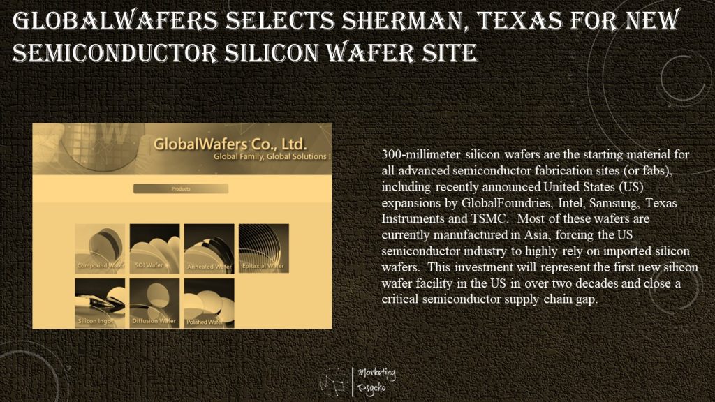
GlobalWafers Selects Sherman, Texas for New Semiconductor Silicon Wafer Site
Taiwan-based global semiconductor silicon wafer company, GlobalWafers, announced that it plans to build a state-of-the-art 300-millimeter silicon wafer factory in Sherman, Texas, which is the first of its kind in the USA over twenty years. Construction is expected to commence later this year.
This 300-millimeter greenfield investment is consistent with the Company’s announcement on February 6th of this year of brownfield and greenfield expansions totaling NTD 100 bn. This new Texas investment could also support as many as 1,500 jobs with production volumes ultimately reaching 1.2 m wafers per month after multiple stages of equipment installation, in alignment with market demand.
300-millimeter silicon wafers are the starting material for all advanced semiconductor fabrication sites (or fabs), including recently announced United States (US) expansions by GlobalFoundries, Intel, Samsung, Texas Instruments and TSMC. Most of these wafers are currently manufactured in Asia, forcing the US semiconductor industry to highly rely on imported silicon wafers. This investment will represent the first new silicon wafer facility in the US in over two decades and close a critical semiconductor supply chain gap.
GlobalWafers Chairman/CEO Doris Hsu stated, “With the global chips shortage and ongoing geopolitical concerns, GlobalWafers is taking this opportunity to address the United States semiconductor supply chain resiliency issue by building an advanced node, state-of-the-art, 300-millimeter silicon wafer factory. Instead of importing wafers from Asia, GlobalWafers USA (GWA) will produce and supply wafers locally thereby reducing significant carbon footprint benefitting both customers and GWA in the current ESG tide worldwide.”
“Today’s announcement from GlobalWafers is critical to rebuilding the domestic semiconductor supply chain, strengthening our economic and national security, and creating U.S. manufacturing jobs,” said U.S. Secretary of Commerce Gina Raimondo. “The Biden Administration has worked tirelessly to make the U.S. an attractive place to manufacture semiconductors and their components, and are excited that GlobalWafers chose Texas for their new facility. But we are at a make-or-break moment to expand domestic semiconductor production. Semiconductor firms need to make investment decisions by the Fall to meet the enormous increased demand for chips. GlobalWafers committed to the US because they believe Congress will get the Bipartisan Innovation Act over the finish line in the coming weeks. Moving quickly to pass this bill will demonstrate America’s commitment to robust domestic semiconductor capacity and provide more companies throughout the supply chain the confidence they need to move forward with investments here.”
“The State of Texas continues to attract and support world-class manufacturers that are leading breakthroughs in innovation and technology,” said Governor Abbott. “GlobalWafers’ ongoing partnership with the City of Sherman, which was initiated with GlobiTech, will create more than a thousand new jobs for the region and investing billions of dollars into our state’s economy, boosting Texas’s global position in the semiconductor industry amid a worldwide chip shortage. We look forward to continuing working with GlobalWafers to keep providing economic opportunities through its expanded presence in the Lone Star State.”
“Sherman has spent years building a business-friendly climate and laying the groundwork to support large employers,” said David Plyer, Mayor of Sherman. “Now, for the second time in less than a year, that investment has paid huge dividends. GlobalWafers’ decision to locate their state-of-the-art, semiconductor silicon wafer facility in Sherman will meet a critical industry need and cement our city’s status as a center of high-tech manufacturing, not only in Texas, but across the country. I want to thank GlobalWafers for their investment in Sherman and for the trust they have placed in our local leadership. This project will provide profound benefits for our citizens, our city and Grayson County for decades to come.”
Production from the first fab is anticipated as early as 2025, according to the Company. GlobalWafers will use the new North Texas site to address the silicon wafer shortage, which has contributed to the semiconductor or “chips” crisis. The company’s business is unprecedented and continues to sell out future output, including the volumes anticipated from this new site.
“This announcement is another critical step in addressing the US and global chips supply issue”, commented Sherman-based, GlobalWafers President Mark England. Moreover, in order to level the global incentive playing field, the impending passage of the US CHIPS Act will be instrumental in ensuring ongoing semiconductor investments of this kind. With the proper level of federal incentives, I can envision the City of Sherman developing into the complete semiconductor ecosystem to fully support the growing US semiconductor industry.”
Navitas Acquires VDD Tech to Expand High-Power, Next-Gen Semiconductor Capabilities
Navitas Semiconductor, the industry-leader in gallium nitride (GaN) power integrated circuits (ICs) has announced the acquisition of VDD Tech, creator of advanced digital-isolators for next-generation power conversion.
Advanced digital-isolation techniques are essential to deliver size, weight, and system-cost improvements in high-power markets such as consumer, motor drive, solar, data center, and EV. VDD Tech’s proprietary modulation-technique enables stable, reliable, efficient power conversion at MHz+ switching speeds.
Proprietary dV/dt sensing, blanking, and refresh technologies enable an unprecedented combination of very-high-voltage-isolation capability with the highest frequency of operation requiring 5-10x higher dV/dt immunity than legacy Silicon. Low isolation-capacitance (<0.5pF) and innovative, robust modulation deliver low-jitter digital-communication for isolated-driver control and analog-sensing feedback. A minimum 200 V/ns Common-Mode Transient Immunity (CMTI) is uniquely guaranteed across all temperature and operating conditions.
VDD Tech was founded in Mont-Saint-Guibert, Belgium, by Vincent Dessard, quickly joined by Aimad Saib, each of them holding a doctorate and 15+ years’ experience in analog / mixed-mode IC research and development. Dessard and Saib have taken leading roles in Navitas’ advanced R&D teams.
“It’s exciting to see two breakthrough technologies – optimized digital-isolators and GaN power ICs – combine to deliver such leading-edge, high-power solutions,” said Dessard, adding “High-speed and high-reliability are the critical factors to accelerate wide-band-gap-semiconductor adoption over legacy silicon-chips, and we’re very excited to be a catalyst in this once-in-a-generation revolution, with new, high-power products launching in 2023.”
“VDD Tech’s isolation technology is a key part of our growing power-and-control integration strategy, creating an additional $1B/yr market opportunity,” said Gene Sheridan, Navitas CEO and co-founder. “We continue to research and review new technologies that we could add to Navitas’ core strengths, and deliver significant CO2 emission-reduction benefits as we continue our mission to ‘Electrify Our World™.”
STMicroelectronics and GlobalFoundries to advance FD-SOI ecosystem with new 300mm manufacturing facility in France
STMicroelectronics, a global semiconductor leader serving customers across the spectrum of electronics applications, and GlobalFoundries Inc., a global leader in feature-rich semiconductor manufacturing, announced they have signed a Memorandum of Understanding to create a new, jointly-operated 300mm semiconductor manufacturing facility adjacent to ST’s existing 300mm facility in Crolles, France. This facility is targeted to ramp at full capacity by 2026, with up to 620,000 300mm wafer per year production at full build-out (~42% ST and ~58% GF).
ST and GF are committed to building capacity for their European and global customer base. This new facility will support several technologies, in particular FD-SOI-based (Fully Depleted Silicon On Insulator) technologies, and will cover multiple variants. This includes GF’s market leading FDX technology and ST’s comprehensive technology roadmap down to 18nm, which are expected to remain in high demand for Automotive, IoT, and Mobile applications for the next few decades.
FD-SOI technology has origins in the Grenoble (France) area. It has been part of ST technology and product roadmap in its Crolles facility since the early beginnings, and it was later enabled with differentiation and commercialized for manufacturing at GF’s Dresden facility. FD-SOI offers substantial benefits for designers and customers, including ultra-low power consumption as well as easier integration of additional features such as RF connectivity, mmWave and security.
ST and GF will receive significant financial support from the State of France for the new facility. This facility will strongly contribute to the objectives of the European Chips Act, including the goal of Europe reaching 20% of worldwide semiconductor production by 2030. In addition to the sizeable, multi-year investment in advanced semiconductor manufacturing in Europe, it will support the leadership and resilience of the European technology ecosystems, from R&D (with the recently announced cooperation on R&D among ST, GF, CEA-Leti and Soitec) to large-volume manufacturing, and support European and global customers with additional capacity in complex, advanced technologies for key end-markets including automotive, industrial, IoT, and communication infrastructure. The new manufacturing facility will be a substantial contributor to global digital and green transformations – delivering key enabling technologies and products. It will generate additional employment at the ST Crolles site (approximately 1,000 additional staff for the new manufacturing facility) and across its ecosystem of partners, suppliers and stakeholders.
By working together, ST and GF will leverage the economies of scale at the Crolles site as they accelerate semiconductor capacity the world needs with high capital efficiency.
“This new manufacturing facility will support our $20 billion+ revenue ambition. Working with GF will allow us to go faster, lower the risk thresholds, and reinforce the European FD-SOI ecosystem. We will have more capacity to support our European and global customers as they transition to digitalization and decarbonization” said Jean-Marc Chery, President and CEO of STMicroelectronics. “ST is transforming its manufacturing base. We already have a unique position in our 300mm wafer fab in Crolles, France which will be further strengthened by today’s announcement. We continue to invest into our new 300mm wafer fab in Agrate (near Milan, Italy), ramping up in H1 2023 with an expected full saturation by end 2025, as well as in our vertically integrated silicon carbide and gallium nitride manufacturing.”
“Our customers are seeking broad access to 22FDX® capacity for auto and industrial applications. The new facility will include GF dedicated foundry capacity for our customers offering GF’s unique innovation and will be managed by GF personnel onsite. This jointly operated, new manufacturing capacity expansion leverages ST’s Crolles existing facility infrastructure enabling GF to accelerate our growth while benefiting from economies of scale to deliver additional capacity in a highly capital efficient manner on our differentiated 22FDX platform, that has shipped more than one billion chips. With today’s announcement, we are expanding GF’s presence within Europe’s dynamic technology ecosystem and reinforcing our position as the leading semiconductor foundry in Europe,” said Dr. Thomas Caulfield, CEO GF. “Our global footprint enables GF to not only meet our customers capacity needs but also provides them supply chain security. The partnership investment with the French government, along with our long-term customer agreements, creates the right economic model for GF’s investment.”
GaN Webinar Series by EPC
Efficient Power Conversion (EPC) webinars represent over 60 years of combined experience in advanced power management technology. From understanding critical design aspects to GaN power device reliability to identifying the value of GaN in specific applications such as high-density computing, ultra-thin laptops, automotive systems, and satellites.
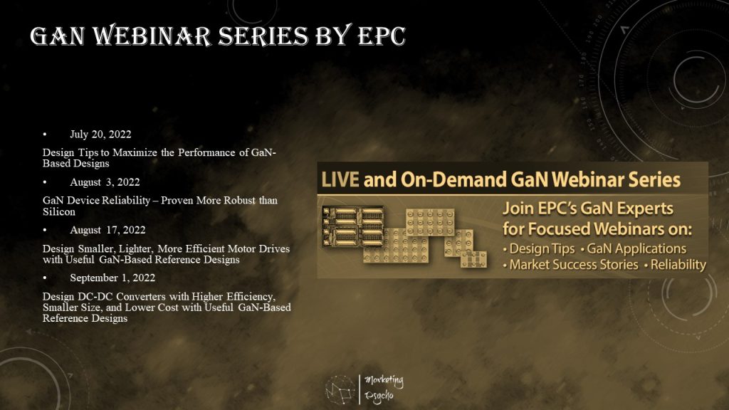
Join the EPC GaN Experts this summer for a series of intensive webinar trainings focused on design techniques to achieve maximum performance in your GaN designs. Each session will last one hour including time for Q&A sessions with GaN Experts. Webinars will take place bi-weekly throughout July and September and topics will include design tips, GaN device reliability, motor drive reference designs, and DC-DC converter reference designs.
Register for the following events:
- July 20, 2022
Design Tips to Maximize the Performance of GaN-Based Designs
- August 3, 2022
GaN Device Reliability – Proven More Robust than Silicon
- August 17, 2022
Design Smaller, Lighter, More Efficient Motor Drives with Useful GaN-Based Reference Designs
- September 1, 2022
Design DC-DC Converters with Higher Efficiency, Smaller Size, and Lower Cost with Useful GaN-Based Reference Designs
Infineon Webinar: High-Power Semiconductor Solutions for Green Hydrogen Electrolyzer Applications
As a leading manufacturer of power semiconductors for wind power and photovoltaic inverters, Infineon also drives renewable power generation. For the production of green hydrogen, very high direct currents (DC) are required in the electrolysis process. The alternating current (AC) supplied by the power grid must first be converted to DC, a process known as rectification or AC-DC conversion. Infineon offers ready-to-use rectifier semiconductor solutions for this purpose.
Infineon provides high-power semiconductors from Infineon for this conversion. Multiple synchronized high-power switches enable high combined system power (> 50 MW). If the electrolysis process is based on electricity from solar panels (which generate DC), only the DC voltage needs to be adjusted. The new thyristor stack design incorporates features necessary for water electrolysis and thus hydrogen production. The stacks are designed as half-bridges and can be used for complete B6C and B12C rectifier circuits. A system power of 10 MW rectifier power can be generated with three half-bridges. With this design, customers do not need to worry about semiconductor and fuse selection as they are already tested and certified.
This webinar will teach why the pre-defined thyristor stack solution is the optimal choice to enter the rectifier market and learn about optimized IGBT power modules for AC- and DC-coupled electrolyzer applications.
Key Take-Aways:
- Gain insights into different use-cases of the production of green hydrogen
- Discover Infineon’s product offering for green hydrogen production
- Explore the advantages of using ready to use thyristor-stack designs for hydrogen generation
- Learn about power module solutions for controlling MW DC-coupled electrolyzer applications
- Date: July 21, 2022
- Time: 3 PM CEST
- Duration: 1 hour
SEMIKRON Webinar: Power Module Reliability: Humidity
High humidity environments present a relatively common, but not well understood, problem for power electronics.
Properly addressing seemingly random humidity-induced failures requires an understanding of both of the environment around a power semiconductor module and the high-risk operating conditions. If you work on the design or field service of outdoor power electronics systems, join this SEMIKRON webinar.
Key Take-Aways:
- Understand the relationship between temperature and humidity
- See how humidity impacts power semiconductor modules
- Learn how humid conditions arise inside electrical enclosures and how the risk of high humidity can be reduced
- Date: July 26, 2022
- Time: 4 PM CEST
- Duration: 1 hour
Subscribe to Power Semiconductors Weekly and watch it on YouTube every Tuesday.
If you prefer a monthly update about the world of power semiconductors delivered to your e-mail address, please, subscribe to Marketing Psycho Power Semiconductors newsletter.