Power Semiconductors Weekly Vol. 71
Showa Denko’s Program to Develop 8-inch SiC Wafers Selected for NEDO’s Green Innovation Fund Projects
Showa Denko (SDK) proposed its “Project to Develop SiC Wafers Technology for Next-generation Green Power Semiconductors” (hereinafter “the Project”) to New Energy and Industrial Technology Development Organization (NEDO) as a candidate for “Projects to Develop Wafers Technology for Next-generation Power Semiconductors” which was set as a research and development target of “Next-generation Digital Infrastructure Construction” in “Green Innovation Fund Projects” (hereinafter GI Fund Projects). And the Project has been selected for GI Fund Projects by NEDO.
In October 2020, the Japanese Government declared that it aims to achieve carbon neutrality by 2050. Aiming to significantly accelerate efforts toward structural changes in the energy and industrial sectors and undertake bold investment for innovation, which are necessary for achievement of the above national target, Ministry of Energy, Trade and Industry (METI) decided in October 2020 to develop a Green Innovation Fund at the level of 2 trillion yen as part of the NEDO. The plan of GI Fund Projects, which are based on the specific goals shared by public and private sectors, is to continuously support companies and other organizations, which show their commitment to challenge such ambitious goals as their business issues ranging from research and development (R&D) to demonstrations to social implementation of the outcomes.
SDK’s business to manufacture SiC epitaxial wafers for power semiconductors (hereinafter SiC epi-wafers) has conducted business transactions with leading power semiconductor manufacturers inside and outside Japan, and has the global-top share in the SiC epi-wafers market. In the Project, SDK plans to make the most of its resources including intelligent property portfolio and development know-how, develop SiC epi-wafers with a diameter of 8 inches, and reduce density of deficiencies by one digit or more, thereby reducing production cost of next-generation power semiconductors. This time, NEDO highly appreciated SDK’s aggressive proposal and its SiC epi-wafers business’s good performance. As a result, NEDO selected SDK’s proposal for GI Fund Projects. The Project’s implementation period will be 9 years, from fiscal 2022 to fiscal 2030. In the Project, SDK will develop technology to accelerate growth rate of SiC bulk single crystal in cooperation with the National Institute of Advanced Industrial Science and Technology (AIST).
The Showa Denko Group aims to be a “Co-Creative Chemical Company” and contribute to the sustainable development of global society. Under this vision, SDK positions its operation to produce SiC epitaxial wafers, which contributes to efficient use of energy, as a next-generation business, and will allocate much of our business resources. The Group will continue contributing to the spread of SiC power semiconductors by maintaining “Best in Class” as its motto and continuing provision of high-performance and highly-reliable products.
Hon Hai, YAGEO to Jointly Participate in XSemi’s Capital Increase for a Private Placement in Taiwan MOSFET Leader APEC
Hon Hai Technology Group and YAGEO Group jointly announced to participate in XSemi Corporation (“XSemi”)’s NT$3.1 billion capital increase. XSemi together announced to participate in the NT$2.8868 billion private placement in the leading Taiwan MOSFET manufacturer Advanced Power Electronics Corp., becoming the largest shareholder with 35 million shares, or 30.08% of the company. After this round of the financing, Hon Hai will become the majority owner of XSemi with 51% holdings, while YAGEO and its related companies will have 49%. At the same time, Hon Hai’s Chairman Young Liu and YAGEO’s Chairman Pierre Chen are nominated to become XSemi’s Chairman and Vice Chairman, respectively, effective as of today.
XSemi is a Hsinchu based joint venture established in the third quarter of 2021, between the world’s largest EMS provider Hon Hai and the global leading electronic component solution provider YAGEO. It is an IC design company specializing in analog and power semiconductors, primarily focusing on the automotive and industrial sectors. The goal of the JV is to serve the strategic system customers and distributors around the world for both Hon Hai and YAGEO.
Hon Hai has more than 40% market share in EMS, which has the tier one brand customer’s base. YAGEO is the only top global passive component solution provider with a leading position in all of resistors, capacitors, and inductors, and its premium distribution channel has the most extensive reach with very high market penetration. These customers of both Hon Hai and YAGEO make up for a strong demand of analog and power semiconductors, and this is one of the key value propositions of XSemi. XSemi is currently leveraging off its internal design capabilities and strategic alliances with many semiconductor leaders in the industry on product designs, capacity planning, distribution channels to enhance XSemi’s product portfolio and market position in analog and power semiconductors. With the strategic collaboration with APEC, XSemi will be able to expedite its business development and strengthen its ability to provide customers with a steady, highly reliable, comprehensive product solutions and services.
Since 2020, before the formation of the JV in 2021, the world has seen an unprecedented market dynamic in the semiconductor world, driven by the combination of short-term supply shocks and rising secular demand. New market opportunities like EV, digital health, robotics, and work-from-home continue to emerge. Leveraging off the strategic collaboration with APEC for its comprehensive MOSFET product line with over 1,000 SKUs, XSemi will be able to expedite its business development and strengthen its product portfolio and customer reach. APEC’s products will also complement highly with XSemi’s internally developed power management IC, SiC chips and modules as total solutions to provide to not only Hon Hai and YAGEO’s existing and future customers, but will also benefit APEC’s current customers greatly. Moreover, APEC will benefit from Hon Hai’s EV footprints and YAGEO’s premium channels to enter the automotive supply chain, to capture more and greater growth opportunities.
“Semiconductor has been one of the three key technology pillars of Hon Hai. To meet the strategic development of 3+3, in the past year we have sped up our progress in semiconductor through Hon Young’s SiC fab and the BOL (Build-Operate-Localize) model to push for fab capacity partnerships and collaborations with automotive players on MCU and SoC. On top of XSemi’s participation through its analog and power products on the auto collaborations, its power module has also shown great progress. With the private placement of APEC, XSemi will be able to fill the gap in its low to high voltage silicon MOSFET product line, and this will provide steady semiconductor supply for the two groups’ future strategic focus in industrial and automotive” said Hon Hai Chairman Young Liu.
“Our alliance with APEC is to capture the upcoming opportunities in analog and power semiconductors. Once the products are ready, we believe that we can quickly deliver them to the customers through YAGEO’s extensive global channels. This approach fits YAGEO’s strategy perfectly which is to continue to provide our global customers with comprehensive electronic component solutions” said YAGEO Chairman Pierre Chen.
Building on top of Hon Hai and YAGEO’s long term strategy and objectives, XSemi will continue to expand its product portfolio and strengthen its product competitiveness to meet the needs of the existing and future customers of the two groups. XSemi aims to be one of the key global analog and power semiconductor providers.
RS Semiconductor Materials Groundbreaking Ceremony of New Factory Construction for 300mm Silicon Wafer
ShanDong GRINM RS Semiconductor Materials Co., Ltd. held a groundbreaking ceremony of new factory construction in Shandong Province, China. The company is currently conducting R&D Business for mass production of 300mm prime wafer and 300mm Wafer Reclaim Business.
The new factory will be constructed as a new manufacturing base for the above two businesses. In the future, the company is aiming to produce 300,000 wafers per month for 300mm prime wafers and 100,000 wafers per month for the 300mm reclaimed wafers.
Siemens Mobility and Mitsubishi Electric Europe B.V. Sign MoU to Push the Use of High Voltage SiC Technology
Siemens Mobility and Mitsubishi Electric Europe B.V. have signed a Memorandum of Understanding (MoU) to cooperate in the field of SiC power module technology with the aim of enabling efficient and sustainable transportation and electrical energy savings in the transportation sector.
With creation of the “European Green Deal”, the EU has committed itself to being the first continent to achieve climate neutrality by 2050, meaning no net emissions of greenhouse gases by 2050. At an intermediate stage, emissions are already to be reduced by 55 % by 2030 compared with 1990. The European Green Deal will result in binding directives for individual sectors regarding CO2 emissions.
These directives apply in particular to the transport sector, where greenhouse gas emissions are to be reduced by 90 % by 2050, alongside an increasing demand for mobility. In particular the rail industry and its suppliers, and more specifically the technologies and components used in rail transport, are important contributors to achieving this goal.
Power semiconductors play a key role in railway vehicles, from trams to high-speed trains. Standard silicon-based power semiconductors are being continuously developed, and new technologies are being advanced, such as the use of SiC (silicon carbide), which will enable even greater efficiency and the greatest reduction in weight in future. It is in fact the railroad market that is stimulating demand for more efficient energy conversion technology.
Mitsubishi Electric’s SiC devices have proven long-term reliability in the most demanding of applications such as traction inverters in trains. The potential for energy savings through the use of Mitsubishi Electric’s wide range of SiC power devices in railway technology exists particularly in the area of traction drives. In particular the full SiC 3300 V power modules contribute to energy saving and the downsizing of traction inverters. The suitable SiC chipset for high-speed switching is used in the standardized LV100 package, which provides low stray inductance and easy paralleling capability. The power losses of LV100 full SiC modules can be reduced by approximately 75 % compared to the conventional Si power modules during the inverter operation. As a result, the efficiency of the traction inverter is increased.
Siemens has always been a pioneer in the construction of electrically powered trains. Their 140 years of experience forms the basis for the new Mireo Plus regional train platform, which enables operators to run their operations efficiently and economically without local CO2 emissions. Using the innovative technology of the battery powered Mireo Plus, Siemens Mobility enables electrification of railway lines even without a continuous overhead contact line. SiC technology is particularly beneficial for regional trains with an innovative battery hybrid drive for use on rail sections with, or without an overhead contact line. It reduces weight to a minimum, optimizes performance, and boosts the efficiency of multiple units in terms of mileage and range. With an energetically optimized drive system, the energy absorption from the grid is nearly 10 percent less than that of today’s vehicles, thanks to the use of SiC components. SiC’s greatest potential is in its higher energy efficiency and reduced weight.
Texas Instruments Breaks Ground on New 300-mm Semiconductor Wafer Fabrication Plants in Sherman, Texas
Texas Instruments (TI) broke ground on its new 300-mm semiconductor wafer fabrication plants (or “fabs”) in Sherman, Texas. In a groundbreaking ceremony attended by elected officials and community leaders, TI Chairman, President and CEO Rich Templeton celebrated the start of construction on the largest private-sector economic investment in Texas history and reiterated the company’s commitment to expanding its internal manufacturing capacity for the long term.
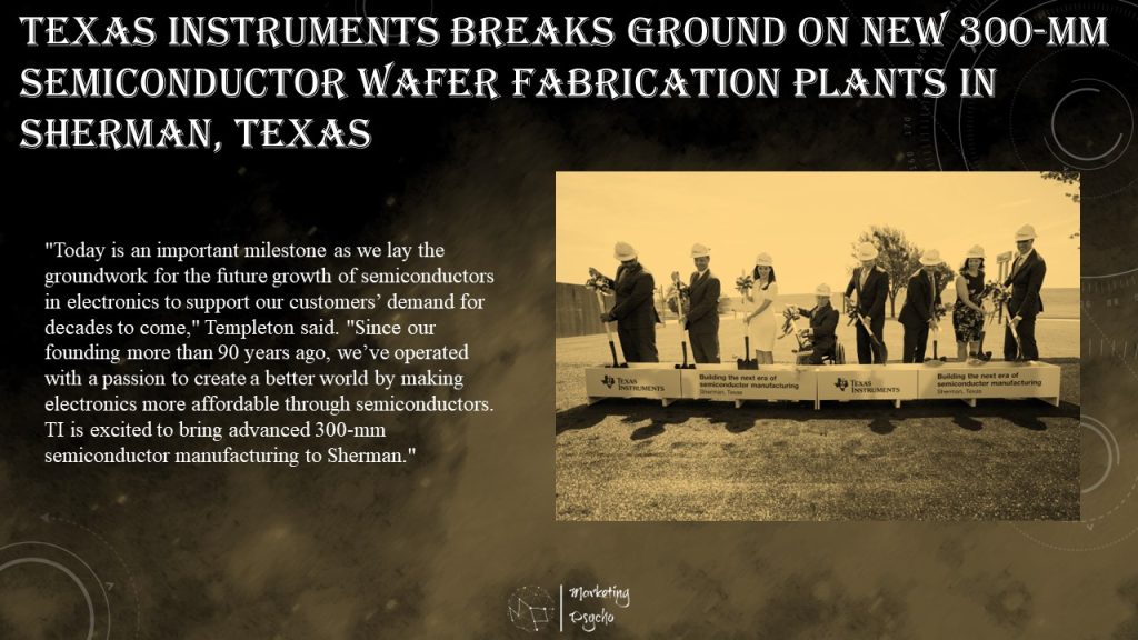
“Today is an important milestone as we lay the groundwork for the future growth of semiconductors in electronics to support our customers’ demand for decades to come,” Templeton said. “Since our founding more than 90 years ago, we’ve operated with a passion to create a better world by making electronics more affordable through semiconductors. TI is excited to bring advanced 300-mm semiconductor manufacturing to Sherman.”
The potential $30 billion investment includes plans for four fabs to meet demand over time, supporting as many as 3,000 direct jobs. The new fabs will manufacture tens of millions of analog and embedded processing chips daily that will go into electronics everywhere.
“This groundbreaking marks the next era of semiconductor production in Sherman that promises to create decades of economic opportunity and improve the quality of life for the region,” said David Plyler, mayor of Sherman. “We are grateful for TI’s long and continued investment in Sherman and look forward to our continued partnership.”
TI has a long-standing commitment to responsible, sustainable manufacturing. The new fabs will be designed to meet one of the Leadership in Energy and Environmental Design (LEED) building rating system’s highest levels of structural efficiency and sustainability: LEED Gold. Advanced 300-mm equipment and processes in Sherman will further reduce waste, water and energy consumption.
Production from the first Sherman fab is expected in 2025. The fabs will complement TI’s existing 300-mm fabs, which include DMOS6 (Dallas), RFAB1 and the soon-to-be-completed RFAB2 (both in Richardson, Texas), which is expected to start production later this year. Additionally, LFAB (Lehi, Utah) is expected to begin production in early 2023. “These investments in long-term manufacturing capacity further extend the company’s cost advantage and provide greater control of our supply chain,” Templeton said.
Innoscience and WPG Sign Worldwide Distribution Agreement
Innoscience Technology, a company founded to create a global energy ecosystem based on high-performance, low-cost gallium-nitride-on-silicon (GaN-on-Si) power solutions, has signed a global distribution agreement with WPG Holdings (WPG), giving customers in all parts of the world access to Innoscience’s leading high and low voltage normally-off (enhancement mode) GaN HEMTs.
Dr Denis Marcon, General Manager, Innoscience Europe comments: “Our aim is to ensure that every power electronics designer – no matter where they are based – can benefit from the efficiency, power and size advantages that GaN technology brings. That is why we have invested in huge capacity – the largest in the world. Distribution is also a big part of our plans, and we are excited and honored to announce WPG – the world’s largest semiconductor distributor – as our first global supply chain partner.”
Adds Nigel Watts, VP, WPG EMEA: “GaN is set for explosive growth as all markets – consumer, communications, automotive, industrial – experience the leap forward in end-product performance they can achieve by switching from traditional silicon-based power devices to GaN. Innoscience is the world’s largest 8-inch GaN-on-Si device manufacturer with a capacity of 10,000 8-inch wafers per month (WPM) – which is set to grow to 70,000 WPM by 2025.
Therefore, it is fitting that Innoscience have signed a global franchise deal with WPG. Product is available NOW and lead-times are far better than the traditional Silicon alternatives. Design now and manufacture sooner.”
EBV Elektronik Webinar: Energy Storage Systems Powered by CoolSiC™
With the enormous amount of energy being consumed in today’s world and government policies to minimize carbon emissions, the shift to renewable energy makes reliably delivering energy where and when it is needed more challenging than ever. As a result, the global demand in residential and commercial for energy storage systems is significantly increasing.
Energy storage systems offer a wide range of technological approaches to manage our supply-demand situation, create a more resilient energy infrastructure, and deliver cost savings for utilities and consumers. Infineon’s CoolSiC™ technology helps reduce energy losses, enabling higher power density and potentially convection cooling.
In this webinar, you will get a deeper insight into Infineon’s comprehensive solution offering for Energy Storage Systems, with a focus on silicon carbide and its important contribution to reducing losses by 50%. You will also get an overview of the structure of energy storage systems and learn more about topologies and implementation approaches.
Key Takeaways:
- Get an overview of the application trends in the ESS market
- Understand different topologies of AC to DC coupled
- Explore the benefits CoolSiC™ can provide in ESS applications
- Gain deeper insights into Infineon’s comprehensive CoolSiC™ portfolio
- Date: June 2, 2022
- Time: 3 PM CEST
- Duration: 1 hour
Subscribe to Power Semiconductors Weekly and watch it on YouTube every Tuesday.
If you prefer a monthly update about the world of power semiconductors delivered to your e-mail address, please, subscribe to Marketing Psycho Power Semiconductors newsletter.