Power Semiconductors Weekly Vol. 69
Power Integrations Launches SCALE EV: Automotive-Qualified IGBT/SiC Module Driver Family
Power Integrations, the leader in gate driver technology for medium- and high-voltage inverter applications, announced the SCALE EV family of gate-driver boards for Infineon EconoDUAL modules. Suitable for original, clone and new SiC variants, the driver targets high-power automotive and traction inverters for EV, hybrid and fuel-cell vehicles including buses and trucks as well as construction, mining and agricultural equipment.
SCALE EV board-level gate drivers incorporate two reinforced gate-drive channels, associated power supplies and monitoring telemetry. The new boards are automotive-qualified and ASIL B certified, enabling implementation of ASIL C traction inverter designs. The first SCALE EV family member to be released is the 2SP0215F2Q0C, designed for the EconoDUAL 900 A 1200-volt IGBT half-bridge module.
Peter Vaughan, director of automotive business development at Power Integrations, said: “Gate-driver design is critical to both the performance and reliability of electric vehicles. By offering a product where the development, testing and qualification plus ASIL certification have already been done, we are dramatically reducing development time and cost.”
The high level of integration provided by innovative new driver ICs enables the entire driver board, including gate power, to fit onto the outline of the power module, while still providing the spacing necessary for reinforced isolation according to the IEC 60664 standard. The ASIC package provides 11.4 mm of creepage and clearance, specifically designed to meet the requirements for 800‑volt vehicle system voltages. Input and output lines to the system microcontroller are connected via two independent on-board connectors to meet functional safety requirements. A single 5 V supply per channel is required, with other isolated voltages being generated on the board itself.
The SCALE EV gate-driver family is rated at 1200 V for 400-volt and 800-volt systems and supports both silicon carbide (SiC) MOSFETs and silicon IGBTs. The design carries a 5500-meter altitude rating and is optionally available with conformal coating for technical cleanliness requirements. The design includes a wide range of protection provisions, including active short-circuit, active discharge of connected DC-link capacitor, overvoltage limitation via active gate control, diagnostic function such as gate monitoring, signal transmission monitoring and on-chip temperature monitoring, and short-circuit and over-current response of less than one microsecond for SiC MOSFETs and less than three microseconds for IGBTs.
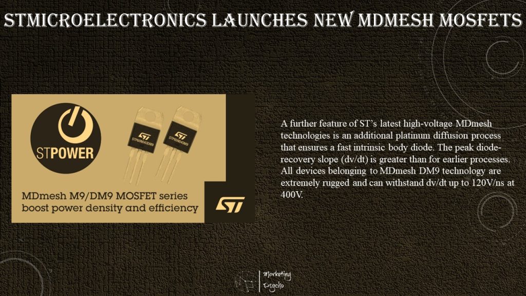
STMicroelectronics Launches New MDmesh MOSFETs
STMicroelectronics’ STPOWER MDmesh M9 and DM9 N-channel super-junction multi-drain silicon power MOSFETs are ideal for switched-mode power supplies (SMPS) in applications from data-center servers and 5G infrastructure to flat-panel televisions.
The first devices to be launched are the 650V STP65N045M9 and the 600V STP60N043DM9. Both have very low on-resistance (RDS(on)) per unit area, which maximizes power density and permits compact system dimensions. Each has the best maximum RDS(on) (RDS(on)max) in its category, at 45mΩ for the STP65N045M9 and 43mΩ for the STP60N043DM9. With very low gate charge (Qg), typically 80nC at 400V drain voltage, these devices have the best RDS(on)max x Qg figure of merit (FoM) currently available.
The gate threshold voltage (VGS(th)), typically 3.7V for the STP65N045M9 and 4.0V for STP60N043DM9, minimizes both turn-on and turn-off switching losses compared with the earlier MDmesh M5 and M6/DM6. The MDmesh M9 and DM9 series also feature a very low reverse recovery charge (Qrr) and reverse recovery time (trr), which further contribute to improved efficiency and switching performance.
A further feature of ST’s latest high-voltage MDmesh technologies is an additional platinum diffusion process that ensures a fast intrinsic body diode. The peak diode-recovery slope (dv/dt) is greater than for earlier processes. All devices belonging to MDmesh DM9 technology are extremely rugged and can withstand dv/dt up to 120V/ns at 400V.
STMicroelectronics Cooperates with SEMIKRON to Integrate SiC Power Technology in Next-Gen EV Drives
STMicroelectronics, a global semiconductor leader serving customers across the spectrum of electronics applications, has revealed it is supplying silicon carbide (SiC) technology for the eMPack® electric-vehicle (EV) power modules from Semikron, one of the world’s leading manufacturers of power modules and systems.
This is the result of a four-year technical collaboration between the two companies to design-in ST’s advanced SiC power semiconductors for superior efficiency and industry-benchmark performance in more compact systems. SiC is quickly becoming the automotive industry’s preferred power technology for EV traction drives, contributing to greater driving range and reliability. Semikron recently announced it had secured a billion-Euro contract to supply their innovative eMPack power modules to a major German car maker, beginning in 2025.
“ST’s industry-leading SiC device-manufacturing capabilities and in-depth expertise with the technology enabled us to integrate these cutting-edge semiconductors with our advanced manufacturing processes, which enhance reliability, power density, and scalability to meet the needs of the automotive industry,” said Karl-Heinz Gaubatz, Semikron Chief Executive Officer (CEO) and Chief Technical Officer (CTO). “As we now move towards volume-production, our collaboration with ST brings the assurance of a robust supply chain that gives control over quality and delivery performance.”
“Leveraging our SiC technology, Semikron’s advanced scalable eMPack family of power modules is ready to make a major contribution towards zero-emission motoring,” said Edoardo Merli, Power Transistor Sub-Group General Manager and Executive Vice President of STMicroelectronics. “In addition to its transformative effect in e-mobility, our SiC technology, now in its third generation, is driving increased efficiency, performance, and reliability in sustainable energy and industrial power-control applications.”
ST’s advanced third-generation SiC technology delivers industry-leading process stability and performance. Engineers from ST and Semikron cooperated to integrate the advanced STPOWER SiC MOSFETs, which control power switching in the main EV traction inverter, with Semikron’s innovative fully sintered Direct Pressed Die (DPD) assembly process. DPD enhances module performance and reliability and enables cost-effective power and voltage scaling. Leveraging the parameters of ST’s SiC MOSFETs, supplied as bare dice, Semikron has established 750V and 1200V eMPack platforms, addressing applications from 100kW to 750kW and battery systems from 400V to 800V.
ST has a broad portfolio of STPOWER SiC MOSFETs in production now. They are available in standard power packages or as bare dice that are optimal for advanced modules where high power density handling is a key requirement. Please contact your local ST sales representative for samples and pricing requests.
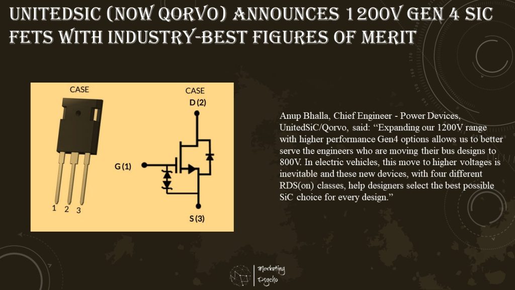
UnitedSiC (now Qorvo) Announces 1200V Gen 4 SiC FETs with Industry-best Figures of Merit
Qorvo®, a leading provider of innovative RF solutions that connect the world, announced a next-generation series of 1200V Silicon Carbide (SiC) Field Effect Transistors (FETs) with industry-leading figures of merit in on-resistance. The new UF4C/SC series of 1200V Gen 4 SiC FETs are ideally suited for mainstream 800V bus architectures in onboard chargers for electric vehicles, industrial battery chargers, industrial power supplies, DC/DC solar inverters, as well as welding machines, uninterruptible power supplies, and induction heating applications.
Anup Bhalla, Chief Engineer – Power Devices, UnitedSiC/Qorvo, said: “Expanding our 1200V range with higher performance Gen4 options allows us to better serve the engineers who are moving their bus designs to 800V. In electric vehicles, this move to higher voltages is inevitable and these new devices, with four different RDS(on) classes, help designers select the best possible SiC choice for every design.”
Highlighting the new UF4C/SC series are the following best-in-class SiC FET figures of merit:
| Figure of Merit | Value |
| RDS(on) • A | 1.35 mOhm-cm2 |
| RDS(on) • Eoss | 0.78 Ohm-uJ |
| RDS(on) • Coss,tr | 4.5 Ohm-pF |
| RDS(on) • Qg | 0.9 Ohm-nC |
All RDS(on) options (23, 30, 53 and 70 milliohm) are offered in the industry standard 4-lead kelvin source TO-247 package, providing cleaner switching at higher performance levels. The 53 and 70 milliohm devices are also available in the TO-247 3-lead package. This series of parts have excellent reliability, based on the well-managed thermal performance, which is a result of an advanced silver-sinter die attach and advanced wafer-thinning process.
All 1200V SiC FETs are included in FET-Jet Calculator™, a free online design tool that allows for instant evaluation of efficiency, component losses, and junction temperature rise of devices used in a wide variety of AC/DC and isolated/non-isolated DC/DC converter topologies. Single and paralleled devices may be compared under user-specified heat-sinking conditions to enable optimum solutions.
Qorvo’s Silicon Carbide and power management products charge, power and control a wide range of industrial, commercial and consumer applications.
Infineon Expands CoolSiC™ Portfolio
The increasing demand for high-power density is pushing developers to adopt 1500 V DC link in their applications to increase the rated power-per-inverter and reduce system costs. However, 1500 V DC based systems also pose more challenges on the system design, such as fast switching at high DC voltage, which typically requires a multi-level topology. This leads to a complicated design and a relatively high number of components. To address this challenge, Infineon Technologies AG introduced its expanded CoolSiC™ portfolio with high-voltage solutions to provide the foundation for next-generation photovoltaic, EV charging and energy storage systems.
The extended CoolSiC portfolio offers 2 kV silicon carbide (SiC) MOSFETs, along with a 2kV SiC diode for applications up to 1500 V DC. The new SiC MOSFET combines both low-switching losses and high-blocking voltage in one device that can optimally meet the requirements of 1500 V DC systems. The new 2 kV CoolSiC technology offers a low drain-source on resistance (R DS(on)) value. In addition, the rugged body diode is suitable for hard switching. The technology enables sufficient overvoltage margin and offers ten times lower FIT rate caused by cosmic ray, compared to 1700 V SiC MOSFETs. Furthermore, the extended gate voltage operating range makes the devices easy to use.
This new SiC MOSFET chip is based on Infineon’s advanced SiC MOSFET technology named M1H which has recently been introduced. The latest advancements enable a significantly larger gate voltage window that improves the on-resistance for a given die size. Simultaneously, the larger gate voltage window provides a high robustness against driver- and layout-related voltage peaks at the gate, without any restrictions even at high switching frequencies. Infineon offers a range of EiceDRIVER™ gate drivers with functional isolation of up to 2.3 kV to support the 2 kV SiC MOSFETs.
onsemi Unveils World’s First TOLL-packaged 650 V Silicon Carbide MOSFET
onsemi, a leader in intelligent power and sensing technologies announced the world’s first TO-Leadless (TOLL) packaged silicon carbide (SiC) MOSFET. The transistor addresses the rapidly growing need for high-performance switching devices that are suitable for designs with high levels of power density. Until recently, SiC devices had been supplied in D2PAK 7-lead packages which required significantly more space.
With a footprint of just 9.90 mm x 11.68 mm, the TOLL package offers 30% savings in PCB area over a D2PAK package. And at a profile of just 2.30 mm, it occupies 60% less volume than a D2PAK package.
In addition to its smaller size, the TOLL package offers better thermal performance and lower package inductance (2 nH) than a D2PAK 7-lead. Its Kelvin source configuration ensures lower gate noise and lower switching losses – including a 60% reduction in turn-on loss (EON) when compared to a device without a Kelvin configuration, ensuring significant improvements in efficiency and power density in challenging power designs as well as improved EMI and easier PCB design.
“The ability to deliver highly reliable power designs in a small space is becoming a competitive advantage in many areas, including industrial, high performance power supplies and server applications,” said Asif Jakwani, senior vice president and general manager, Advanced Power Division, onsemi. “Packaging our best-in-class SiC MOSFETs in the TOLL package not only reduces space but enhances performance in many areas such as EMI and reduces losses. The result is a highly reliable and rugged high-performance switching device that will help power designers meet their stringent power design challenges.”
SiC devices offer significant advantages over their silicon predecessors, including enhanced efficiency at high frequencies, lower EMI, higher temperature operation and greater reliability. onsemi is the only supplier of silicon carbide solutions with vertical integration capability including SiC boule growth, substrate, epitaxy, device fabrication, best-in-class integrated modules and discrete package solutions.
The first SiC MOSFET to be offered in the TOLL package is the TBL045N065SC1 which is intended for demanding applications including switch-mode power supplies (SMPS), server and telecommunication power supplies, solar inverters, uninterruptible power supplies (UPS) and energy storage. The device is suitable for designs that are required to meet the most challenging efficiency standards including ErP and 80 PLUS Titanium.
The NTBL045N065SC1 has a VDSS rating of 650 V with a typical RDS(on) of just 33 mΩ and a maximum drain current (ID) of 73 A. Based upon wide bandgap (WBG) SiC technology, the device has a maximum operating temperature of 175°C and ultra-low gate charge (QG(tot) = 105 nC) that significantly reduces switching losses. Additionally, the TOLL package is MSL 1 (moisture sensitivity level 1) rated – and guaranteed – to ensure that failure rates in mass production are reduced.
In addition, onsemi offers automotive grade devices with TO-247 3 lead, 4 leads and D2PAK 7 leads packages.
Keysight Technologies Delivers Next-Generation Power Device Analyzer / Double-Pulse Tester
Keysight Technologies, Inc., a leading technology company that delivers advanced design and validation solutions to help accelerate innovation to connect and secure the world, announced the new PD1550A Advanced Dynamic Power Device Analyzer, a next-generation Double-Pulse Tester (DPT) with enhanced capabilities that enable customers to test entire power modules faster and easier than ever before.
Power modules are used in various applications such as electric vehicles (EV), solar power inverters, trains, home appliances and aircraft due to ease of design, high energy density and reliability. New, wide-bandgap (WBG) device-based power modules are now used by designers to take advantage of the device’s fast-switching operation, reducing the size of the power electronic module, and ensuring efficiency. However, WBG power modules also introduce test challenges that require new solutions to properly characterize these devices while eliminating failed prototypes and reducing design cycles.

Introduced in 2019, Keysight’s PD1500A Power Device Dynamic Analyzer / Double-Pulse Tester was the first complete solution for discrete WBG power device characterization and is now used by power converter designers and power semiconductor manufacturers around the world. Now, the new PD1550A expands beyond the PD1500A’s capabilities to offer the first complete integrated solution that tests entire power modules (up to 1360 V, up to 1000 A). As a result, automotive original equipment manufacturers (OEMs), Tier 1 suppliers and power converter designers can test faster and gain more insights into power module characteristics, enhancing the safety and reliability of power circuits for automotive applications.
Keysight’s PD1550A Advanced Dynamic Power Device Analyzer tests wide-bandgap power modules to deliver faster, more insightful testing and accelerate time to market.
“Leveraging Keysight’s measurement expertise enables us to provide customers focused on power semiconductor components and power modules with a high-performance and double-pulse test solution,” said Thomas Goetzl, vice president and general manager for Keysight’s automotive & energy solutions business unit. “The new PD1550A expands our offering into whole power module testing, which is used in high-power converter designs, while maintaining ease-of-use and compliance to worldwide safety regulations.”
Keysight’s PD1550A delivers an off-the-shelf, turn-key system that easily tests discrete devices and power modules with minimal setup requirements. It is fully certified to worldwide safety regulations and is calibrated and tested as a system, offering customers the following key benefits:
- Delivers repeatable, reliable measurements while simplifying and automating the testing processes.
- Eliminates the need for customers to build, test, certify and maintain an in-house system.
- Provides accurate gate voltage characteristics on high-side device using True Pulse Isolated Probe Technology.
- Ensures accurate high current measurement with high-bandwidth RF compensation.
- Includes interface board with solderless contact and exchangeable gate resistor technologies.
- Minimizes costs and accelerates time to market by reducing design time and number of prototypes needed.
- Working with customers, Keysight can customize the system to their specific needs, especially the pin and pad layouts.
Subscribe to Power Semiconductors Weekly and watch it on YouTube every Tuesday.
If you prefer a monthly update about the world of power semiconductors delivered to your e-mail address, please, subscribe to Marketing Psycho Power Semiconductors newsletter.