Power Semiconductors Weekly Vol. 62
Infineon Presents Optimized CoolSiC™ MOSFETs 650 V in D²PAK
Megatrends like digitalization, urbanization, and electromobility lead to increased power consumption. At the same time, energy efficiency is getting more and more important. Infineon Technologies AG responds to these megatrends and resulting demands by offering a new family of CoolSiC™ 650 V silicon carbide (SiC) MOSFETs to deliver reliable, easy-to-use, and cost-effective top performance. The devices build on Infineon’s state-of-the-art SiC trench technology and come in a compact D2PAK SMD 7-pin package with .XT interconnection technology. They target high power applications including servers, telecom, industrial SMPS, fast EV charging, motor drives, solar energy systems, energy storage, and battery formation.
The new products offer improved switching behavior at higher currents and 80 percent lower reverse recovery charge (Q rr) and drain-source charge (Q oss) than the best silicon reference. The reduced switching losses allow high-frequency operations in smaller system sizes, enabling higher efficiency and power density. The trench technology is the basis for superior gate oxide reliability. Together with an improved avalanche and short-circuit robustness this ensures the highest system reliability even in harsh environments. The SiC MOSFETs are suitable for topologies with repetitive hard commutation as well as for high temperature and harsh operations. Thanks to a very low on-resistance (R DS(on)) dependency with temperature they show an excellent thermal behavior.
Featuring a wide voltage from gate to source (V GS) range from -5 V up to 23 V and supporting 0 V turn-off V GS and a gate-source threshold voltage (V GS(th)) greater than 4 V, the new family also works with standard MOSFET gate driver ICs. Additionally, the new products support bi-directional topologies and full dv/dt controllability, offering reduced system cost and complexity, as well as ease of adoption and integration. The .XT interconnection technology significantly improves the package’s thermal capabilities. Up to 30 percent extra loss can be dissipated compared to a standard interconnection. With ten new products, the Infineon D2PAK 7-pin portfolio of SiC MOSFETs is the most granular in the market.
Microchip Unveils Industry-Leading 3.3 kV Silicon Carbide Power Devices
System designers of traction power units (TPUs), auxiliary power units (APUs), solid-state transformers (SSTs), industrial motor drives and energy infrastructure solutions require high-voltage switching technology to increase efficiency, reduce system size and weight and enhance reliability. Microchip Technology Inc. announced the expansion of its SiC portfolio with the release of the industry’s lowest on-resistance [RDS(on)] 3.3 kV SiC MOSFETs and highest current-rated SiC SBDs available in the market, enabling designers to take advantage of ruggedness, reliability and performance. With the expansion of Microchip’s SiC portfolio, designers are equipped with the tools to develop smaller, lighter and more efficient solutions for electrified transportation, renewable energy, aerospace and industrial applications.
Many silicon-based designs have reached their limits in efficiency improvements, system cost reduction and application innovation. While high-voltage SiC provides a proven alternative to achieve these results, until now, the availability of 3.3 kV SiC power devices was limited. Microchip’s 3.3 kV MOSFETs and SBDs join the company’s comprehensive portfolio of SiC solutions that include 700V, 1200V and 1700V die, discretes, modules and digital gate drivers.
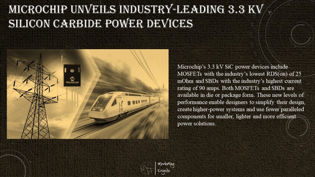
Microchip’s 3.3 kV SiC power devices include MOSFETs with the industry’s lowest RDS(on) of 25 mOhm and SBDs with the industry’s highest current rating of 90 amps. Both MOSFETs and SBDs are available in die or package form. These new levels of performance enable designers to simplify their design, create higher-power systems and use fewer paralleled components for smaller, lighter and more efficient power solutions.
“We focus on developments that provide our customers the ability to quickly innovate systems and move their end products into a competitive advantage position faster,” said Leon Gross, vice president of Microchip’s discrete product business unit. “Our new family of 3.3 kV SiC power products allows customers to move to high-voltage SiC with ease, speed and confidence and benefit from the many advantages of this exciting technology over silicon-based designs.”
Microchip has released hundreds of SiC power devices and solutions to production over the last three years, ensuring designers can find the right voltage, current and package fit for their application requirements. All Microchip SiC MOSFETs and SBDs are designed with customer confidence in mind, featuring industry-leading ruggedness and reliability. The company’s devices are backed by its customer-driven obsolescence practice, which ensures devices will continue to be produced for as long as customers need them, and Microchip can produce them.
Customers can combine Microchip SiC products with the company’s other devices including 8-, 16- and 32-bit microcontrollers (MCUs), power management devices, analog sensors, touch and gesture controllers and wireless connectivity solutions to create complete system solutions at a lower overall system cost.
ROHM Starts Production of 150V GaN HEMTs
ROHM 150V GaN HEMTs, GNE10xxTB series (GNE1040TB) increase the gate withstand voltage (rated gate-source voltage) to an industry-leading 8V – ideally to be applied in power supply circuits for industrial equipment such as base stations and data centers along with IoT communication devices.
In recent years – due to the rising demand for server systems in response to the growing number of IoT devices – improving power conversion efficiency and reducing size have become important social issues that require further advancements in the power device sector.
As GaN devices generally provide higher switching characteristics and lower ON resistance than silicon devices, they are expected to contribute to lower power consumption of various power supplies and greater miniaturization of peripheral components.
Along with mass-producing industry-leading SiC devices and feature-rich silicon devices, ROHM has developed GaN devices that achieve superior high frequency operation in the medium voltage range, allowing us to provide power solutions for a wider variety of applications.
These new products utilize an original structure that raises the rated gate-source voltage from the conventional 6V to 8V. As a result, degradation is prevented, even if overshoot voltages exceeding 6V occurs during switching – contributing to improved design margin and higher reliability in power supply circuits. The GNE10xxTB series is offered in a highly versatile package featuring superior heat dissipation and large current capability, facilitating handling during the mounting process.
ROHM has trademarked GaN devices that contribute to greater energy conservation and miniaturization under the name EcoGaN™, and is working to expand the lineup with devices that improve performance. Going forward, ROHM will continue to develop control ICs that leverage analog power supply technology such as Nano Pulse Control™ and modules that incorporate these ICs, along with power solutions that contribute to a sustainable society by maximizing the performance of GaN devices.
This year, the Ministry of Economy, Trade, and Industry (METI) of Japan has set a target of 30% energy savings for new data centers by 2030 – less than 10 years from now. However, system performance must not only be energy efficient, but also robust and stable as they have become a vital part of our social infrastructure.
In response, ROHM has developed a new GaN device that provides a gate withstand voltage of 8V, the industry’s highest, providing a high degree of robustness and stability while achieving superior energy savings. Beginning with these products, ROHM will continue to improve power supply efficiency in power sources by combining with proprietary Nano Pulse Control™ analog power supply technology, creating a major technological trend that will help the semiconductor and telecommunications industries become carbon neutral by 2040.
EcoGaN™ refers to GaN devices that contribute to energy conservation and miniaturization by maximizing the low ON resistance and high-speed switching characteristics of GaN, with the goals of reducing application power consumption, miniaturizing peripheral components, and reducing design load along with the number of parts required.
Key Features:
- Original structure extends the rated gate-source voltage to 8V
Existing GaN devices with a withstand voltage of 200V or less typically have a rated gate-source voltage of 6V with respect to a gate drive voltage of 5V, resulting in an extremely narrow voltage margin of just 1V. Exceeding the rated voltage can cause reliability problems such as degradation and destruction, plus the gate drive voltage requires high accuracy control, which has been a major obstacle to the popularization of GaN devices.
In response, this new series succeeds in raising the rated gate-source voltage from the typical 6V to an industry-leading 8V by adopting an original structure. This expands the voltage margin during device operation, so even if a voltage overshoot exceeding 6V occurs during switching, the device will not degrade, contributing to higher reliability of the power supply circuit.
- Optimized package provides excellent heat dissipation and supports large currents
The GNE10xxTB series utilizes a highly versatile package with a proven track record for reliability and mountability that delivers superior heat dissipation and large current capability, facilitating handling during the mounting process. What’s more, using copper clip junction packaging technology reduces parasitic inductance by 55% over conventional packages, maximizing device performance when designing circuits for high frequency operation.
- Achieves over 96.5% power supply efficiency in the high frequency band
These new products maximize device performance by increasing the rated gate-source voltage and adopting a low-inductance package, achieving a high efficiency of 96.5% or more in the high 1MHz frequency band, contributing to improved efficiency and greater miniaturization in power supply equipment.
Application Examples:
• 48V input buck converter circuits for data centers and base stations
• Boost converter circuits for the power amp block of base stations
• LiDAR drive circuits, wireless charging circuits for portable devices
• Class D audio amps
New SBD & MOSFET Packages from Wolfspeed Slash Size, Increase Power Density
Size matters in almost any application, as does efficiency. For instance, in enterprise data centers, a significant portion of the upfront costs are due to building floor space, and most operational costs are from utility electricity. Or consider the very different industrial power and motor-drive applications in which careful trade-offs among size, weight, efficiency, and cost are needed for success.
Indeed, the pressure to improve power density is only increasing. Traditional data centers that use about 10 kW per rack are no longer sufficient for demanding end-use applications like high-performance computing, artificial intelligence, and machine learning.
A similar trend is true for industrial applications, wherein increasing demand for smaller size and weight and lower cooling requirements requires higher efficiency and higher power density.
Wide-bandgap semiconductor technologies, like Wolfspeed’s Silicon Carbide (SiC) MOSFETs and Schottky Barrier Diodes (SBDs), allow power designers to utilize several advantages compared with silicon. Lower conduction and switching losses increase efficiency, and high-frequency operation helps reduce the size of passive components — inductors, capacitors, and transformers. Their high-junction–temperature capabilities allow the use of smaller thermal management solutions. By supporting high-voltage operation, such as 650 V or more, Wolfspeed’s products also help reduce the number of switches required in high-voltage applications.
The net result is improved system-level efficiency and power density at lower system-level cost.
These advantages, however, put pressure on packaging technology so that it capably supports device performance rather than hinders it. Common packaging challenges include:
• Keeping parasitics in check
• Reducing package size without sacrificing thermal performance
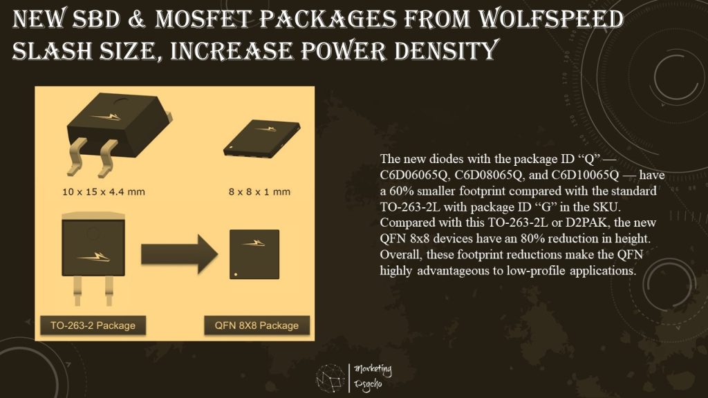
To address market demand for high power density, Wolfspeed has introduced new, smaller surface-mount packages for its discrete SiC Schottky diodes and MOSFETs. The company’s C6D 650 V SiC Schottky diodes are now available in QFN 8 × 8 and their C3M SiC discrete MOSFETs are now sampling in a TO lead-less (TOLL) package that is considerably smaller than the other options of TO-247-3, TO-247-4, and TO-263-7.
Traditional through-hole packages, such as the TO-247, can pose assembly automation challenges for some high-volume system producers. If all devices on the board are surface-mount (SMDs), assembly can be accomplished in a single automated step. This has a significant impact toward reducing production costs.
The new diodes with the package ID “Q” — C6D06065Q, C6D08065Q, and C6D10065Q — have a 60% smaller footprint compared with the standard TO-263-2L with package ID “G” in the SKU. Compared with this TO-263-2L or D2PAK, the new QFN 8×8 devices have an 80% reduction in height. Overall, these footprint reductions make the QFN highly advantageous to low-profile applications.
The SiC SBD technology also enables a low forward-voltage drop (VF) of 1.27 V at 25˚C and 1.37 V at 175˚C, thereby reducing forward power losses. This allows designers to achieve the highest possible system-level efficiencies in applications like PFC boost converters.
The QFN package offers a lower lead inductance, which is critical to reducing switching losses in the final system and enabling high-frequency operation. By allowing higher switching frequencies, the parts enable higher power densities to be achieved. The QFN packages also incorporate efficient thermal management with bottom-side cooling.
All devices feature a creepage distance that is suitable for applications with an operating voltage of 400 V. The parts offer continuous forward current (IF) ratings of 6 A, 8 A, and 10 A and junction-to-case thermal resistance (Rθ, JC) as low as 1.4˚C/W.
The surface-mount TOLL is an innovative package that the industry is adopting typically for high-current, high-power–density applications. Wolfspeed’s industrial-application–qualified 650 V SiC MOSFETs in the TOLL package are significantly smaller than other package options. Compared with the standard TO-263-7L’s footprint of 151.5 mm2 and height of 4.30 mm, the TOLL device has a footprint of 113 mm2 and height of 2.2 mm. That is a nearly 25% reduction in footprint and an even more remarkable 50% reduction in height.
Wolfspeed’s TOLL package also features a low source inductance that allows designers to utilize lower external gate resistance, which not only reduces the switching losses but helps avoid peak voltage overshoots during turn-off. The parts are therefore well-suited to high switching frequency applications, which can help increase power density by reducing the size of magnetic components.
To address thermal management requirements from a package of this size, the new TOLL devices have much larger back metal tabs to help lower device junction temperature (Tjmax). In thermal simulations the package was tested for dissipating 28 W with convection cooling at 5,000 W/m2K. The TOLL device could keep Tjmax as low as 152˚C compared with TO-263-7L’s 175˚C. Designs using these devices would therefore require less thermal management, granting cost, space, and weight benefits to the application.
The TOLL devices also have a minimum creepage of 3.5 mm (D-S) that is ideal for ~400VDC operation. The MOSFETs — PC3M0045065L, PC3M0060065L, and PC3M0120065L — are offered in three RDS(ON) options of 45 mΩ, 60 mΩ, and 120 mΩ, with rated drain currents (ID) of 50 A, 36 A, and 21 A, respectively.
This makes the switches suitable for a wide range of applications, including server/telecom power supplies, consumer/computing/industrial SMPS, solar power inverters, motor drives, light EVs, battery chargers, and home appliances.
Wolfspeed’s new SMD power devices not only save precious application space but dissipate heat more efficiently, which helps deliver on lower production costs, lower thermal solution costs, and higher power densities.
NXP and Hitachi Energy Collaborate on Power Module to Accelerate Silicon Carbide Adoption in E-mobility
NXP® Semiconductors has announced a collaboration with Hitachi Energy to accelerate the adoption of silicon carbide (SiC) power semiconductor modules in e-mobility. The project aims to provide more efficient, reliable and functionally safe SiC MOSFET-based solutions for powertrain inverters comprised of NXPs advanced, high-performance GD3160 isolated HV Gate Drivers and Hitachi Energy’s RoadPak automotive SiC MOSFET power modules.
Compared to traditional silicon IGBTs, SiC MOSFET power devices offer electric vehicle makers the ability to increase the range and overall efficiency of their systems. SiC MOSFET power devices, enabled by high-performance power semiconductor modules and isolated gate drivers, offer faster switching speeds, lower turn-on resistance and reduced thermal dissipation that can help drive down the size and cost of an electric vehicle’s (xEV’s) powertrain inverter and lower the required capacity of the battery pack, extending the vehicle’s range.
Hitachi Energy’s high-performance automotive power semiconductor module RoadPak delivers excellent heat dissipation, low stray inductances, and long-term ruggedness to withstand the challenging automotive environment; a key to unleashing the full capabilities and benefits of SiC MOSFETs. To attain optimal performance, the power module is paired with NXP’s GD3160 high-voltage, isolated gate driver which enables fast and reliable switching and fault protection.
“Working with Hitachi Energy has allowed us to highlight the efficiency and range benefits of SiC MOSFETs for e-mobility. By pairing the GD3160 with the Hitachi Energy’s RoadPak SiC module, we’ve delivered a solution that aims to reduce the transition time from evaluation to performance optimization of SiC MOSFETs used in traction inverters.” – Robert Li, Vice President and General Manager of NXP’s Drivers & Energy Systems Product Line

Hitachi Energy has been leveraging its technology and the experience gained in the industrial and transportation segments to develop its high-density RoadPak automotive SiC power modules for e-mobility applications. The RoadPak half-bridge power module incorporates 1200V SiC MOSFETs, integrated cooling pin-fins and low inductance connections all in a small form factor. It can support applications from e-buses and electric passenger vehicles to high-performance Formula-E race cars.
“We are pleased to be collaborating with NXP Semiconductors to improve the performance of e-mobility with faster and low-loss switching. Our joint solution based on NXP Gate Units and SiC RoadPak from Hitachi Energy, built on our industry-leading experience and innovative technologies, will help enable e-vehicles to drive longer distances, thus helping to reduce global carbon emissions and power sustainable transportation everywhere.” – Rainer Kaesmaier, Managing Director of Hitachi Energy’s Semiconductor business
The FRDMGD31RPEVM, the GD3160 half-bridge EVB customized for the RoadPak SiC module is available now. The Hitachi Energy’s 1200V RoadPak half-bridge SiC module is available now in 580A, 780A, and 980A options.
Navitas Announces World’s First 20-Year Warranty for GaN ICs
Navitas Semiconductor, the industry-leader in gallium nitride (GaN) power integrated circuits has announced a breakthrough 20-year limited warranty for its GaNFast technology – 10x longer than typical silicon, SiC or discrete GaN power semiconductors – and a critical accelerator for GaN’s adoption in data center, solar and EV markets.
GaN is a next-generation semiconductor technology that runs up to 20x faster than legacy silicon chips. Navitas’ proprietary GaNFast™ power ICs integrate GaN power (FET) and GaN drive plus control, sensing and protection. The result is easy-to-use, high-speed, high-performance ‘digital-in, power-out’ building blocks that deliver up to 3x faster charging in half the size and weight, and with up to 40% energy savings compared with earlier silicon solutions.
The unprecedented 20-year limited warranty is founded on Navitas’ holistic approach to product reliability through design, testing, characterization and certification. As the pioneer in GaN power ICs and a founding member of the industry’s JEDEC JC-70.1 GaN standards committee, Navitas developed proprietary high-speed production and qualification testing to set new standards in GaN reliability.
“With over 40 million units shipped, 174 billion hours in the field and zero reported GaN-related field failures, plus 5.8 billion equivalent device hours testing, Navitas is now able to offer a 20-year warranty for GaNFast power ICs,” said Anthony Schiro, Navitas’ VP Quality and Sustainability. “As we describe in our sustainability report, each GaN IC saves 4 kg of CO2. So, the faster customers can adopt GaN, the better it will be for our environment. GaN could save up to 2.6 Gtons CO2 per year by 2050.”
Navitas is the industry-leader in fast and ultra-fast chargers for consumer mobile applications with customers including Samsung, Dell, Lenovo, Xiaomi, OPPO, LG and Motorola. With dedicated design centers for data center and EV, plus availability of high-power GaNFast power ICs, Navitas’ high-volume production quality and commitment to long-term reliability accelerate the adoption of next-gen GaN technology.
“As leading-edge customers like Enphase (solar), Brusa (EV) and Compuware (data center) confirm GaN’s technical and environmental benefits over legacy silicon chips, they are laser-focused on critical, long-term reliability,” said Gene Sheridan, CEO and co-founder of Navitas. “GaN power ICs have a 6x-lower FIT rate (failures in time) than silicon, and this 20-year limited warranty puts Navitas front and center in the next-generation semiconductor revolution.”
The 20-year limited warranty applies to all packaged Navitas GaNFast power ICs in mass production. Terms and conditions apply.
Power Integrations Unveils New Office Facility in Switzerland
Power Integrations, the leader in high-voltage integrated circuits for energy-efficient power conversion, opened its newly constructed facility in Biel, Switzerland at a ceremony hosted by the company’s CEO, Balu Balakrishnan, and attended by Biel mayor Erich Fehr. The 4,600-square-meter, $20 million facility is the new home for about 60 engineers and other technology professionals, a number that is expected to rise as the company continues to grow in the years ahead. In addition to modern office and laboratory space, the contemporary building houses a surface-mounted-technology (SMT) line used to develop prototypes for the company’s gate-driver products. The facility also features a 25-kilowatt rooftop solar array.
Power Integrations’ presence in Switzerland dates to its 2012 acquisition of CT-Concept Technologie AG. Its Biel operation specializes in gate drivers for high-power applications such as solar and wind energy, electric locomotives and efficient DC transmission lines, and is an integral part of the company’s efforts in the electric-vehicle market. Worldwide, Power Integrations employs approximately 770 people, with additional R&D centers at its Silicon Valley headquarters as well as in Canada, Malaysia and the United Kingdom, and design-support centers in Germany and the Philippines.
In addition to its innovative gate drivers, Power Integrations is known for high-voltage integrated circuits (ICs) used in power supplies for appliances, smartphones, computers and myriad consumer-electronics and industrial products. The company’s ICs feature proprietary energy-saving technologies such as gallium-nitride transistors and EcoSmart™ technology, which reduces the energy consumed by electronic products in “standby” or idle modes. Reflecting the environmental benefits of the company’s products, the company’s Nasdaq-listed shares are included in clean-technology indexes such as The Cleantech Index and the Nasdaq Clean Edge Green Energy Index. The company shipped nearly two billion ICs and gate drivers in 2021, generating revenues of $703 million—an increase of more than 40 percent from the prior year.
Commented Mr. Balakrishnan: “We are delighted to open our new, permanent home in Biel, bringing all of our local employees under one roof and giving us ample room for the growth we expect in the years ahead. Our presence here is an essential part of our company’s efforts to develop innovative products for a low-carbon future. We are grateful to the city’s leaders for their support of this project, and we look forward to a long and productive future together.”
Biel mayor Erich Fehr commented: “I am pleased by Power Integrations’ enduring commitment to the city of Biel. The fact that such an innovative, fast-growing company has chosen to establish roots here speaks for the attractiveness of our city and our region as a business location. At the same time, our city benefits from Power Integrations’ dynamism and innovation, as the past decade has already proven.”
Power Integrations’ new Swiss home was planned and built by Biel-based architectural firm GLS Architects. Commented Nik Liechti, CEO of GLS Architects: “This has been an exciting project for our firm from its very beginning more than five years ago. We have particularly enjoyed the challenge of integrating a high-tech SMT line into this contemporary office building, and we are extremely proud of the result. The cooperation with Power Integrations and the authorities on this project was excellent and a key factor in the successful development of this high-density building. We were able to meet all deadlines and cost projections despite the difficult circumstances during the pandemic.” Power Integrations –
Subscribe to Power Semiconductors Weekly and watch it on YouTube every Tuesday.
If you prefer a monthly update about the world of power semiconductors delivered to your e-mail address, please, subscribe to Marketing Psycho Power Semiconductors newsletter.