Power Semiconductors Weekly Vol. 59
Infineon Presents New Automotive 750 V EDT2 IGBTs
Infineon Technologies AG is launching the new EDT2 IGBTs in a TO247PLUS package. The devices are optimized for automotive discrete traction inverters and expand Infineon’s portfolio of discrete high-voltage devices for automotive applications. Due to their high quality, the IGBTs meet and exceed the industry standard AECQ101 for automotive components. As a result, the devices can significantly increase the performance and reliability of inverter systems. With the automotive micro-pattern trench-field-stop cell design, the IGBTs are based on a technology that has already been successfully utilized in several inverter modules such as the EasyPACK™ 2B EDT2 or the HybridPACK™.
As required for the target applications, the product family is short-circuit-robust. In addition, the TO247PLUS package offers a greater creepage distance for easy design-in. EDT2 technology is optimized for traction inverter and has a breakdown voltage of 750 V, supporting battery voltages up to 470 V DC, and significantly lower switching and conduction losses.
The rated currents of the discrete EDT2 IGBTs are 120 A and 200 A at 100°C, each with a very low forward voltage, reducing conduction losses by up to 13 percent compared to the previous generation. With a rated current of 200 A, the AIKQ200N75CP2 is also the best-in-class discrete IGBT in a TO247Plus package. Thus, for a defined target power class, fewer devices are needed in parallel. Additionally, power density increases and system costs decrease.
In addition, the EDT2 IGBTs feature an extremely narrow parameter distribution. The collector-emitter saturation voltage (V ce(sat)) difference between typical and maximum values is less than 200 mV and the gate threshold voltage (V GEth) difference is less than 750 mV. Furthermore, the thermal coefficient is positive. Together, this enables easy parallel operation and provides system flexibility and power scalability for final designs. Moreover, the IGBTs offer smooth switching performance, low gate charge (Q G) and a high junction temperature (T vjop) of 175°C.
Toshiba’s New Generation Super Junction Power MOSFET “DTMOSVI Series”
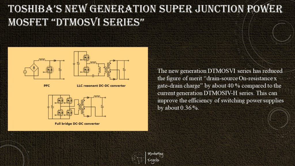
Toshiba Electronic Devices & Storage Corporation has added four products — “TK090E65Z, TK110E65Z, TK155E65Z, and TK190E65Z” — to its DTMOSVI series of 650 V new generation super junction structure N-channel power MOSFETs that are used for switching power supplies of industrial equipment for data centers, power conditioners for photovoltaic generators and so forth. The lineup has been expanded with respect to package, drain-source On-resistance, and gate-drain charge.
The new generation DTMOSVI series has reduced the figure of merit “drain-source On-resistance x gate-drain charge” by about 40 % compared to the current generation DTMOSIV-H series. This can improve the efficiency of switching power supplies by about 0.36 %.
Toshiba will continue to expand its product lineup to meet market trends and help improve the efficiency of power supplies.
Applications:
- Switching power supply for industrial equipment
- Data center (Server, etc.)
- Power conditioners for photovoltaic generators
- Uninterruptible power systems
Features:
- The values of “drain-source On-resistance x gate-drain charge” have been reduced by about 40 % to improve the efficiency of switching power supplies.
- Through hole type of TO-220 package
FormFactor Introduces High-Power Semiconductor Wafer Probing System
FormFactor, Inc., a leading semiconductor test and measurement supplier, introduced the TESLA300 high power semiconductor probing system. Designed specifically for IGBT and power MOSFET device measurements, the TESLA300 provides accurate data at up to 10,000 V and up to 600 A current on 300mm wafers. Integrating new anti-arcing and wafer automation capabilities, the TESLA300 enables high-throughput, unattended testing over a wide thermal range to speed development and lower production cost of power devices.
Key features of the TESLA300 include:
- Accurate, high-yield, drain-to-source resistance (Rds) vertical device measurements over temperature, automated and assured through FormFactor’s unique Contact Intelligence™ technology and powerful Velox 3 engineering software.
- Industry-leading measurement performance, with patented MicroChamber® shielded test environment, and TESLA FemtoGuard™ thermal chuck with AttoGuard® and MicroVac™ technologies for low contact resistance and high temperature uniformity.
- Flexible wafer handling, up to 300mm in wafer size, with semi or fully-automated configuration.
- Full thermal testing from -60 to +300°C.
- Integrated, TÜV-certified safety system for high-voltage measurements.
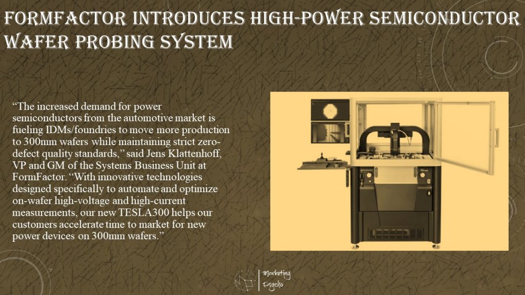
“The increased demand for power semiconductors from the automotive market is fueling IDMs/foundries to move more production to 300mm wafers while maintaining strict zero-defect quality standards,” said Jens Klattenhoff, VP and GM of the Systems Business Unit at FormFactor. “With innovative technologies designed specifically to automate and optimize on-wafer high-voltage and high-current measurements, our new TESLA300 helps our customers accelerate time to market for new power devices on 300mm wafers.”
InventChip Sets Up Strategic Fund Solely Invested by EV Maker Xiaopeng
InventChip Technology, a Chinese semiconductor company that focuses on silicon carbide power devices, has established a strategic fund financed exclusively by new energy vehicle manufacturer Guangzhou Xiaopeng Motors Technology.
The fund will be used to expand the market, for research and development, to retain talent and for investment in operations. No details were given of the amounts involved.
InventChip is the first company in China to develop 6-inch silicon carbide metal oxide semiconductor field effect transistors and has so far shipped 400,000 units. Compared with silicon, silicon carbide consumes less energy. A silicon carbide device that is only a tenth the size of a silicon device delivers the same performance and consumes a quarter of the energy.
With advantages in conversion efficiency, size and heat dissipation, silicon carbide power devices have been widely applied in industrial and photovoltaic fields, said Vice President Zhang Xiaofeng. There will be growing demand in electric drives, on-board chargers and charging piles.
Last October, InventChip raised hundreds of millions of Chinese yuan (equivalent to tens of millions of US dollars) in Series-A+ and Series A++ financing led by private equity firms Lightspeed China Partners, State Development & Investment and Chongqing Xiaomi Venture Capital.
EIB Releases €600 million Loan to STMicroelectronics
The European Investment Bank (EIB) is providing significant financial support to STMicroelectronics: a €600 million loan for the semiconductor group’s research and development (R&D) and pre-industrialization activities in Europe.
The operation concerns investments in R&D activities for innovative technologies and components, as well as in pilot production lines for advanced semiconductors. These investments will be implemented in STMicroelectronics’ existing facilities in Italy (Agrate and Catania) and France (Crolles). They will contribute to the development of technologies and products to address the major challenges of environmental transition and digital transformation in all sectors.
The global semiconductor market is currently worth more than €500 billion and is expected to double by 2030. Europe accounts for around 10% of world production capacity, a sharp decline compared with previous decades (24% in 2000 and 44% in 1990).
The EIB’s support for STMicroelectronics actively contributes to the policies put in place at European level in coordination with the Member States, in order to strengthen the semiconductor industry in Europe, in research and development, design and production and bring public financing to strategic industrial projects. The aim is to support the competitiveness of European players of this key sector, as it affects all industrial sectors, particularly those in which European manufacturers hold leadership positions.
Bruno Le Maire, French Minister for the Economy, Finance and Recovery, said: “There will be no political sovereignty without digital sovereignty. Europe must use all the tools it has, to invest in new technologies. The EIB’s role is crucial, when it grants a €600 million loan to STMicroelectronics. Our goal is clear: to accelerate the production of semiconductors in France and Italy. It is only by mastering this technology, that we will be able to safeguard the European Union’s strategic independence. Those investments contribute more broadly to the support to our new growth model that creates high-value industrial jobs in our countries.”
Daniele Franco, Italian Minister for the Economy and Finance, said: “The semiconductor industry is fundamental for the digital transition of the European Union economies. The support that the EIB provides to STMicroelectronics, one of the world’s most advanced and innovative companies, represents an important step towards strengthening and making the European semiconductor industry more competitive, with a significant impact on employment and growth.”
Jean-Marc Chéry, President and CEO of STMicroelectronics, said: “This new loan from the EIB, with which we have been working in partnership for many years, is complementing the various existing instruments supporting our industry, such as the important projects of common European interest (IPCEI) and others that are currently being set up by the European Commission and the Member States. It is essential to work in Europe on the whole value chain: R&D, design and manufacturing, in collaboration with the different European ecosystems. ST will contribute to the goal of 20% of global production in Europe by 2030 and will continue to develop and manufacture in Europe innovative technologies and products to support the environmental transition and the digital transformation of all industries.”
EIB Vice-President Gelsomina Vigliotti, said: “Semiconductors are the key components without which no digital and ecological transition is possible. Thanks to the long-standing relationship between the EIB and ST, which has resulted in eight financing operations since 1994 worth more than €3,15 billion, the EIB supports Europe’s autonomy, competitiveness and technological sovereignty.”
EIB Vice-President Ambroise Fayolle, said: “Financing innovation, a key factor in European competitiveness and technological sovereignty, is an EIB priority. This €600 million loan to support the R&D efforts of one of Europe’s leading semiconductor companies illustrates Europe’s commitment to this sector, which is crucial to the future of our economies and our strategic autonomy.”
onsemi Divests Wafer Manufacturing Sites as Part of Fab-Liter Strategy
onsemi, a leader in intelligent power and sensing technologies, is executing on its fab-liter manufacturing strategy with the ultimate goal of sustainable financial performance through gross margins expansion.
The company signed an agreement to divest its South Portland, Maine fab. Earlier, onsemi closed on the sale of its wafer fabrication facility in Oudenaarde, Belgium. As onsemi transitions production to more efficient fabs within its network, it will improve its cost structure by eliminating fixed costs associated with the sold fabs and lowering its unit costs.
“The proposed divestitures show that we are well on our way to achieve an optimized manufacturing network while supporting our customers with long-term assurance of supply,” said Hassane El-Khoury, president and chief executive officer of onsemi. “The transactions provide employees at the affected fabs with continued employment and growth opportunities while allowing onsemi to transition production from these fabs to other manufacturing sites in an orderly manner.”
onsemi and Diodes Incorporated entered into a definitive agreement for the divestiture of onsemi’s wafer fabrication facility and operations in South Portland, Maine. Diodes plans to expand on its 200mm wafer fab capacity in support of its analog product growth. The transaction is expected to close in the second quarter of 2022.
On February 8, 2022, onsemi completed the sale of its manufacturing facility in Oudenaarde, Belgium to BelGaN Group BV, a consortium of investors and executives with extensive expertise in semiconductors, BelGaN plans to become a leading 6-inch and 8-inch gallium nitride (GaN) foundry in Belgium.
GaN Power Devices and Applications
Since the 2019 release of the 3rd edition textbook, GaN Transistors for Efficient Power Conversion, published by J. Wiley, there has been rapid adoption of GaN transistors and integrated circuits into a myriad of end-use applications such as robots, drones, AI computers, AC adapters, autonomous vehicles, and even vacuum cleaners.
This book, GaN Power Devices and Applications, provides an update on gallium nitride technology and applications by leading experts. The book starts with two years of new information on technology developments, design techniques, and reliability beginning right after the publication of the 3rd edition textbook. In a practical sense, this book includes detailed descriptions of the latest examples of GaN’s usage in power supplies, lidar, motor drives, and space applications.
Subscribe to Power Semiconductors Weekly and watch it on YouTube every Tuesday.
If you prefer a monthly update about the world of power semiconductors delivered to your e-mail address, please, subscribe to Marketing Psycho Power Semiconductors newsletter.