Power Semiconductors Weekly Vol. 57
Mitsubishi Electric to Launch “SLIMDIP-X” Power Semiconductor Module
Mitsubishi Electric Corporation released its new SLIMDIP-X power semiconductor module, which achieves low thermal resistance and noise for use in home-appliance inverter systems. This new module in the SLIMDIPTM series is expected to help simplify and reduce the size of inverter systems used in products such as air conditioners, washing machines and refrigerators.
Product Features:
- Reduced thermal resistance will contribute to simpler thermal designs
- An upgraded insulation sheet reduces thermal resistance between the chip and case by approximately 35% compared to the existing SLIMDIP-L module, and the rating current has been increased to 20A.
- High-temperature suppression in the reverse-conducting IGBT (RC-IGBT) will help to simplify the thermal designs for inverter systems.
- Low noise will help realize smaller, lower-cost inverter systems
- Noise reduction technology deployed in the RC-IGBT helps to reduce the number of noise suppression components, which will lead to smaller and lower-cost inverter systems.
- SLIMDIP series package compatibility helps to shorten design time
- Adopting a SLIMDIP series-compatible package, including dimensions and pin layout (while nevertheless increasing the rating current), will greatly help to shorten inverter-system designing.
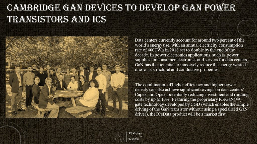
Cambridge GaN Devices to Develop GaN Power Transistors and ICs
Fabless semiconductor company Cambridge GaN Devices Ltd. (CGD) has launched ICeData, a project aiming to develop and commercialize a highly efficient Gallium Nitride (GaN)-based IC (integrated circuit) for use in data center server power supplies.
The primary goal of the ICeData project is to deliver state-of-the-art GaN power IC technology to boost the efficiency of data center server power supplies to more than 98%. Specifically tailored for Switched Mode Power Supplies (SMPS) for data centers and telecommunication servers, ICeData will contribute to the saving of more than 8 megatons (million metric-tons) of CO2 emissions annually in 2030.
Data centers currently account for around two percent of the world’s energy use, with an annual electricity consumption rate of 400TWh in 2018 set to double by the end of the decade. In power electronics applications, such as power supplies for consumer electronics and servers for data centers, GaN has the potential to massively reduce the energy wasted due to its structural and conductive properties.
The combination of higher efficiency and higher power density can also achieve significant savings on data centers’ Capex and Opex, potentially reducing investment and running costs by up to 10%. Featuring the proprietary ICeGaN(™) gate technology developed by Cambridge GaN Devices (which enables the simple driving of the GaN transistor without using a specialized GaN driver), the ICeData product will be a market first.
It will also boast smart features for sensing and protection to enhance reliability, without the need for extra components. The on-chip sensing and protection circuits can react in nanoseconds to overcurrent and overtemperature events, protecting the device and ultimately protecting the power system.
By the project’s end Cambridge GaN Devices will have a qualified and production-ready set of GaN power IC solutions. The overall GaN market is estimated to grow from a few million USD today to more than $1.1 billion by 2026, driven by demand for lighter and efficient power supplies and more compact and powerful on-board chargers for EV and HEV. Cambridge GaN Devices’ first product line featuring ICeGaN(™) technology will be released in the first half of 2022.
GlobalWafers Italian Subsidiary Launches 300mm Expansion Plan
MEMC Electronic Materials SpA Board of Directors, following up GlobalWafers Group Board of Directors decision, approved the expansion of its existing facility located in Novara (Italy), that’s currently producing 200mm silicon wafers, by adding a new 300mm wafers production module.
This investment decision, in line with recent GWC announcement of expanding its presence in Europe thanks to the endorsement of the Italian Government (MISE) the European Union as well as some key European microelectronic device manufacturers, will further strengthen GWC historical presence in Italy where both Merano and Novara facilities are operating since 1974-1976 respectively.
The approved expansion will be concentrated on 300mm polished and epi wafers development and production to be utilized in the most advanced technology applications. Moreover, by mean of this expansion into Italian Piedmont region, GWC will achieve the full 300mm line integration in Italy since 300mm crystal growth new development and expansion was already occurring in its facility located in Merano (BZ).
This advanced 300mm line will be operating starting mid-2023. Mass production will follow according to customers’ qualifications and then first industrial deployment phases to ramp up to the needed volume of the new products being developed and produced by this advanced and fully automated facility.
Given the significant capital associated to the start-up of this new 300mm advanced line, conditions for which the project will become executive are: 1. Financial participation of the partners with whom the project is being developed; 2. Access to the Government/European funds associated to the investments Microelectronic supply chain in Europe/Italy (i.e. IPCEI-ME/CT).
The whole Novara area as well as the Piedmont region will benefit from the spill over of this very advanced technology investment. In this respect, collaborations with very important universities and research centers as well as with microelectronic firms, operating in Europe and abroad, are already in place for guaranteeing the continuous growth of the local semiconductor industry ecosystem that everybody knows it’s strategic for both Italian and European economies.
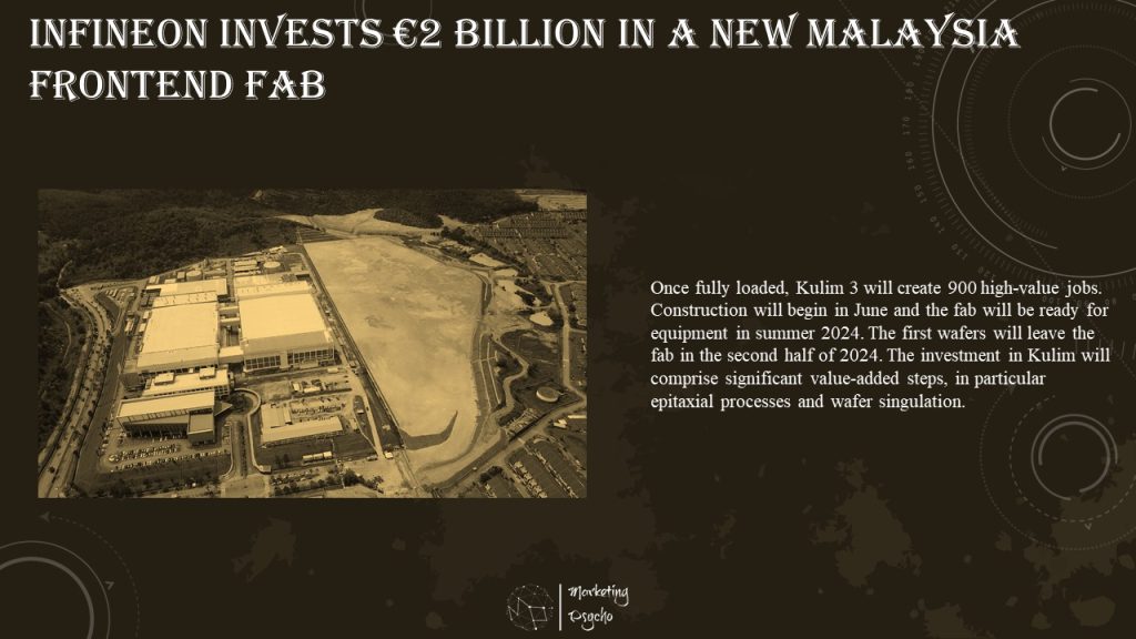
Infineon Invests €2 billion In a New Malaysia Frontend Fab
Infineon Technologies AG is strengthening its market leadership in power semiconductors by adding significant manufacturing capacities in the field of wide bandgap (SiC and GaN) semiconductors. The company is investing more than €2 billion to build a third module at its site in Kulim, Malaysia. Once fully equipped, the new module will generate €2 billion in additional annual revenue with products based on silicon carbide and gallium nitride.
The expansion, following the company’s long-term manufacturing strategy, will benefit from the excellent economies of scale already achieved for 200-millimeter manufacturing in Kulim. It will complement Infineon’s leading position in silicon, based on 300-millimeter manufacturing in Villach and Dresden. The new investment will greatly reinforce the overall competitive advantage, which is based on the combination of technology leadership, a broad product portfolio and deep application know-how, following Infineon’s “Product to System” approach.
“Innovative technologies and the use of green electrical energy are key in reducing carbon emissions. Renewable energies and electro-mobility are major drivers for a strong and sustainable rise in power semiconductor demand,” said Jochen Hanebeck, Chief Operations Officer at Infineon. “The expansion of our SiC and GaN capacity is readying Infineon for the acceleration of wide bandgap markets. We are creating a winning combination of our development competence center in Villach and cost-effective production in Kulim for wide bandgap power semiconductors.”
Infineon already provides SiC-based products to more than 3,000 customers today. Used in a variety of applications, these semiconductors offer added value to the customer because of better system performance in terms of efficiency, size and cost compared to silicon-based solutions. Infineon’s strategic “Product to System” approach also facilitates the adoption of SiC-based semiconductors with leading base technology, the broadest product and package portfolio and unparalleled application know-how. Focus applications are industrial power supply, photovoltaic, transportation, drives, automotive and EV charging. Infineon is targeting revenues of $1 billion with SiC-based power semiconductors by the middle of the decade. The GaN market is also predicted to undergo massive growth – from $47 million in 2020 to $801 million in 2025 (CAGR: 76%; source: Yole – Compound Semiconductor Quarterly Market Monitor Q3 2021). Infineon has leading-edge system and application understanding, a broad GaN IP portfolio and large R&D force.
Once fully loaded, Kulim 3 will create 900 high-value jobs. Construction will begin in June and the fab will be ready for equipment in summer 2024. The first wafers will leave the fab in the second half of 2024. The investment in Kulim will comprise significant value-added steps, in particular epitaxial processes and wafer singulation.
“Malaysia is one of Infineon’s main regional hubs and this further investment truly attests to our conducive ecosystem and the capability of our local talent to support long-term growth”, says Malaysia’s Senior Minister and Minister of International Trade and Industry, Dato’ Seri Mohamed Azmin Ali. “The Government, through Malaysian Investment Development Authority (MIDA), will continue working closely with our strategic investors to solidify Malaysia’s prominence as a key semiconductor hub in the region.”
The Villach site will continue to serve as the innovation base and global competence center for wide bandgap technology by converting existing silicon facilities over the next years. 6” and 8” silicon lines will be converted to SiC and GaN manufacturing by repurposing non-specific silicon equipment. The Villach site is currently preparing for further growth opportunities.
SEMIKRON Secures Billion Euro Contract with German Automotive Manufacturer
SEMIKRON has secured a billion euro contract with a major German car manufacturer for their new power module platform eMPack®. This new platform, which is optimized for silicon carbide technology, will be used in the car manufacturer’s next generation EV inverters.
One of the crucial factors that clinched the deal is SEMIKRON’s fully sintered “Direct Pressed Die “(DPD) technology, which allows for extremely compact, scalable and reliable inverters
Series production is scheduled to begin in 2025. The contract is worth in excess of one billion euros.
Over the past few years, SEMIKRON has unfalteringly pursued its plan to become an automotive supplier, building upon decades of experience in the development and production of power modules.
The strategy SEMIKRON is pursuing here focuses on global megatrends such as zero emission mobility as a means of combatting climate change. In relation to this, the eMobility market will remain one of the fastest growing markets for power semiconductors in the years ahead.
According to business intelligence and strategy research company BIS Research, the number of hybrid and electric vehicles will continue to grow by 23% a year until 2029. And SEMIKRON intends to grow with this market – with the help of its eMPack® power module platform for electric drive systems and full inverter solutions for utility vehicles.
SEMIKRON is well equipped to meet this goal and contribute substantially to the shift to zero-emission and sustainable mobility.
PowerAmerica’s Annual Meeting 2022
PowerAmerica will once again host its annual meeting of SiC and GaN professionals.
The event will offer networking sessions, keynote remarks, industry perspectives, PowerAmerica member-initiated project updates, and SiC and GaN technology roadmap sessions. Engineering and business development professionals are especially encouraged to attend.
Join PowerAmerica March 1-3, 2022 in Raleigh, N.C. for the 2022 PowerAmerica annual meeting, a 2 1/2-day gathering of leaders in the SiC and GaN power electronics field.
Wolfspeed Webinar: Silicon Carbide Solutions for Energy Storage Systems
Wolfspeed Silicon Carbide power devices enable higher performance and lower system cost for energy storage applications. Join their webinar to see how Silicon Carbide MOSFETs can simplify the power topologies required to meet ever-increasing energy efficiency standards, while shrinking system size, weight, and cost.
Whether you’re building a single-phase residential system (5-15 kW) or three-phase commercial system (30-100 kW), Wolfspeed Silicon Carbide solutions are the right choice for system performance and efficiency.
Key Takeaways:
- Overview of energy storage system (ESS) applications where Silicon Carbide power devices can add higher performance and lower system cost
- Common power levels and system topologies
- SiC product fit, component choices using Wolfspeed reference designs to demonstrate performance and cost advantages in actual hardware
- Summary of efficiency, power density, and system cost advantages from using Wolfspeed Silicon Carbide in Energy Storage/UPS designs
- Date: February 24, 2022
- Time: 8 PM CET
- Duration: 1 hour
Subscribe to Power Semiconductors Weekly and watch it on YouTube every Tuesday.
If you prefer a monthly update about the world of power semiconductors delivered to your e-mail address, please, subscribe to Marketing Psycho Power Semiconductors newsletter.