Power Semiconductors Weekly Vol. 56
Mitsubishi Electric to Launch Half-Bridge Driver HVIC with BSD Function
Mitsubishi Electric Corporation announced the coming launch of a half-bridge driver high-voltage (600V) integrated circuit (HVIC) equipped with a built-in bootstrap diode (BSD) function that can help to reduce the number of parts required in inverter systems. The new HVIC, which is designed for circuits that drive power semiconductors in low-capacity inverter systems, will also help to lower the power consumption of white goods, electric bikes and other electrical products. Sales will begin on April 1.
HVICs that drive power semiconductors in inverter systems are in increasing demand for use in motor-control systems that help to save energy and improve the performance of consumer products and industrial equipment.
Product Features:
- Built-in BSD function helps to reduce the number of parts in inverter systems
- Mitsubishi Electric’s new HVIC for inverter systems is equipped with a BSD function that – enables inverter systems and high-voltage wiring to be designed with fewer parts.
- BSD function’s high-voltage metal oxide semiconductor (MOS) achieves high noise resistance
- Mitsubishi Electric’s proprietary high-voltage MOS structure suppresses current leakage during charging.
- The MOS structure is free of parasitic elements that can cause latch-up malfunctions due to noise when switching inverters (negative potential surge noise generated in freewheel diode during reflux mode).
- Compatible with existing M81776FP model
- The new HVIC’s external profile (8-pin small outline package), pin layout and electrical properties are compatible with the existing model (M81776FP) for greatly simplified replacement.
Vishay Intertechnology N-Channel MOSFETs Deliver Best in Class RDS(ON)
Vishay Intertechnology, Inc. introduced two new n-channel TrenchFET® MOSFETs that increase power density, efficiency, and board-level reliability in telecom and industrial applications. To achieve these design goals, the 60 V SiJH600E and 80 V SiJH800E combine ultra-low on-resistance with high temperature operation to +175 °C and high continuous drain current handling. Their space-saving PowerPAK 8x8L package promotes board-level reliability with its bond wireless construction and gullwing leads for mechanical stress relief.
The ultra-low on-resistance of the SiJH600E and SiJH800E — 0.65 mΩ and 1.22 mΩ typical at 10 V, respectively — is 54 % and 52 % lower than same-generation devices in the PowerPAK SO-8. This translates into energy savings by minimizing power losses due to conduction.
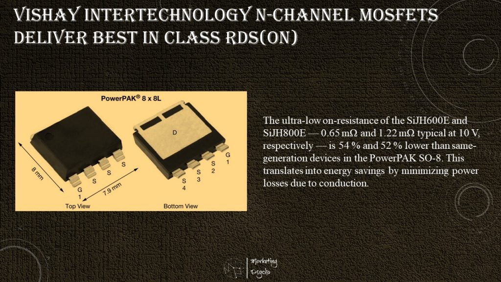
For increased power density, the SiJH600E and SiJH800E deliver continuous drain current of 373 A and 288 A, respectively, in a package that is 60 % smaller and 57 % thinner than the D2PAK. To save board space, each MOSFET can also be used in place of two PowerPAK SO-8 devices in parallel.
Dual High-Side Switches from STMicroelectronics Add Extra Flexibility for Driving Capacitive Loads
STMicroelectronics’ latest high-side switches, the IPS2050H and the IPS2050H-32, permit two programmable current-limit values for smart driving of capacitive loads that draw high startup current.
These new dual-channel switches have an input-voltage range from 8V to 60V and can withstand up to 65V on the input pin, ensuring flexibility and robust performance in industrial applications. The integrated power MOSFET has low Rds(on), resulting in high energy efficiency and low thermal dissipation. In addition, MOSFET single-pulse avalanche energy greater than 1J at 2A boosts reliability for handling inductive loads. There is also an active clamp for fast demagnetization.
The IPS2050H allows the main current limit to be programmed up to 2.5A for driving loads controlled by a PLC module and for use in equipment such as factory automation I/O peripherals, Computer Numerical Control (CNC) machines, and general driving of resistive, inductive, and capacitive loads. The IPS2050H-32 has a higher maximum current limit of 5.7A for use with unidirectional motors in equipment such as vending machines. The current-activation threshold and limit values are configurable using external resistors. An external capacitor sets the duration of the startup current limit for smart driving of capacitive loads.
Extensive built-in protection features and diagnostics enhance safety and reliability, including Under-Voltage Lock-Out (UVLO) and protection against overvoltage, overload, short-circuit, ground disconnection, and Vcc disconnection. Individual fault signaling for each channel indicates over-load and junction over-temperature events. An additional sensor is provided for case over-temperature protection. The switches meet IEC 61000-4-2 ESD, IEC 61000-4-4, and IEC 61000-4-5 specifications for ESD, fast-transient, and surge immunity.
Demonstration boards and software are available to help quickly evaluate the driving and diagnostic capabilities when connected to industrial loads. The boards include X-NUCLEO-OUT03A1 and X-NUCLEO-OUT04A1 digital-output expansion boards for use with STM32* Nucleo development boards, with associated X-CUBE-OUT3, STSW-OUT03F4, and STSW-OUT03G4 software drivers. In addition, STSW-IFAPGUI graphical user interface source code helps users realize an entire industrial automation environment.
European Chips Act
Semiconductors are the building block of all electronic products. They play a central role in modern economies and daily lives. They underpin the digital transformation and are essential to all industries, such as the car industry, communications, data processing, space, defense, smart devices and gaming, to name a few.
The recent global chips shortage has disrupted supply chains, caused product shortages ranging from cars to medical devices, and in some cases even forced factories to close.
The European Chips Act, adopted by the Commission on 8 February 2022, seeks to strengthen the semiconductor ecosystem. It is composed of a Communication, which spells out the European Strategy and rationale behind the Chips Act, a proposal for a Regulation, and a Recommendation to Member States.
The European Chips Act will reinforce the semiconductor ecosystem in the EU, ensure the resilience of supply chains and reduce external dependencies. It is a key step for the EU’s technological sovereignty. And, it will ensure Europe meets its digital decade target of doubling its global market share in semiconductors to 20%.
It will do so by focusing on 5 strategic objectives:
- Strengthening research and technological leadership;
- Building and reinforcing Europe’s capacity to innovate in the design, manufacturing and packaging of advanced chips;
- Putting in place an adequate framework to increase production by 2030;
- Addressing the skills shortage and attracting new talent;
- Developing an in-depth understanding of global semiconductor supply chains.
Toshiba Group Technology Strategy
As detailed in its November announcements, “Transforming Toshiba to Enhance Shareholder Value,” “Notice Regarding Toshiba Group’s Strategic Reorganization” and “Toshiba Announces Strategic Reorganization to Separate into Three Standalone Companies to Enhance Shareholder Value,” Toshiba decided to reorganize into three independent companies by conducting a spin-off of Toshiba’s two core businesses into two new publicly listed companies. Since then, Toshiba has been in talk with a variety of the stakeholders including its shareholders and relevant authorities.
Since this is the first large-scale spin-off transaction in Japan, after the announcement, Toshiba consulted with related parties to confirm the details, and as a result, it turned out there were obstacles which were not initially expected. Therefore, in order to increase the certainty of realization, Toshiba has refined the transaction scheme, while maintaining the fundamental policy of operating the two core business domains independently.
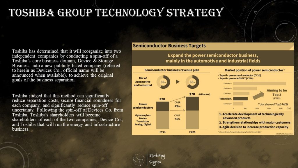
Consequently, Toshiba has determined that it will reorganize into two independent companies by conducting a spin-off of a Toshiba’s core business domain, Device & Storage Business, into a new publicly listed company (referred to herein as Devices Co., official name will be announced when available), to achieve the original goals of the business separation.
Toshiba judged that this method can significantly reduce separation costs, secure financial soundness for each company, and significantly reduce spin-off uncertainty. Following the spin-off of Devices Co. from Toshiba, Toshiba’s shareholders will become shareholders of each of the two companies, Device Co., and Toshiba that will run the energy and infrastructure business.
Toshiba Device & Storage Business plans to:
- Focus on expanding their semiconductor business mainly in automotive and industrial fields
- Double R&D for power semiconductors to strengthen technological superiority and accelerate product development
- Strengthen relations with major customers
Find the complete business strategy here – Business Strategy of Device Co.
GlobalWafers Capacity Expansion
GlobalWafers Co., Ltd. announced investment plans after its voluntary all-cash tender offer for the outstanding ordinary shares of Siltronic AG failed to reach all completion conditions, in particular all regulatory approvals, by the final deadline of January 31, 2022. The proceeds originally intended for the acquisition are now earmarked for capital and operating expenses. GlobalWafers foresees total capital expenditures of New Taiwan dollar (NTD) 100 billion (approx. USD 3.6 billion) from 2022 to 2024, including substantial greenfield investments.
Doris Hsu, Chairperson and CEO of GlobalWafers, commented: “While the failed completion of our offer for Siltronic is disappointing we have pursued a dual-track strategy from the very beginning of the tender offer. I am very excited that we can consider now a broad range of options to advance technology development and enhance our capacities.”
GlobalWafers now considers a number of brown- and greenfield capacity expansion plans, including 300mm wafer and Epitaxial wafer (EPI), 200mm and 300mm Silicon on Insulator wafers (SOI), 200mm Float-Zone wafers (FZ), Silicon carbide (SiC) wafers (including SiC Epi), Gallium Nitride on Silicon wafers (GaN on Si) and other large-size next-generation products. The expansion plan includes investments across Asia, Europe and the United States of up to NTD 100 billion spanning both brownfield and greenfield projects. The new production lines are expected to ramp up in the second half of 2023 and to be expanded on a quarterly basis.
GlobalWafers shall focus on strengthening its growth by building new production lines, which specialize in next-generation products for advanced processes targeting large-size wafers and compound semiconductors. Wafers for advanced processes will play a larger role in the product spectrum of GlobalWafers, thus further optimizing its product mix. GlobalWafers will be ahead of its peers for mass production of new products in order to capture timely the new business opportunities from innovative end applications, enhance its first mover advantage, increase revenue scale and expand business territory for the benefits of its customers and shareholders.
Nexperia – Five Years of Independence
Nexperia celebrates five years since entering the semiconductor industry as an independent entity. During this time, the Nexperia brand, while still relatively young, has become firmly established in the marketplace by building on the foundations of a strong track record in semiconductor manufacturing over several decades.
Right from the start back in 2017, Nexperia combined passion with professionalism and set about growing with its customers by providing them with the innovative products that they need. It now celebrates five years of forward thinking, growth, and market-leading products. During this time Nexperia has also developed industry-leading capacity that consistently meets the highest automotive standards, while also providing the widest range of discrete components, power, and Logic ICs.
While justifiably proud of its past achievements, Nexperia is a future focused company with renewed ambition and commitment to further innovation and progress, both for itself and its customers. With a world-class team that includes a visionary CEO and forward-thinking leaders, Nexperia is aggressively targeting an increased market share by seizing on new opportunities as they emerge. “We will have record investments into our facilities, people and into innovative products in 12 inch. This will enable Nexperia to transition into a world leader in essential semiconductors with a revenue of more than USD $10bn by 2030”, says Xuezheng Zhang, CEO of Nexperia. “We will achieve this by becoming the number one supplier in the market segments that we serve.”
Nexperia’s continued growth can be attributed to ongoing investment in products, production facilities and above all, people – TeamNexperia. It is investing heavily in manufacturing facilities in Europe and Asia and continuously expanding capacity. Nexperia recently opened new R&D design centers in Penang, Malaysia and Shanghai, China and it will soon open a new design center in Dallas, USA. Nexperia is seeking to recruit new talent to become part of and contribute to its ongoing success. This success of Nexperia’s investments is evidenced by a continuous growth in revenues during its first five years.
Subscribe to Power Semiconductors Weekly and watch it on YouTube every Tuesday.
If you prefer a monthly update about the world of power semiconductors delivered to your e-mail address, please, subscribe to Marketing Psycho Power Semiconductors newsletter.