Power Semiconductors Weekly Vol. 52
Toshiba Expands Power MOSFETs Lineup
Toshiba Electronic Devices & Storage Corporation has started mass production of two N-channel MOSFETs using SOP Advance(WF) package for automotive and has expanded its lineup. The two models are 60 V “XPH2R106NC, XPH3R206NC.”
These new products are qualified with the automotive reliability standard AEC-Q101. The package is a surface mount type SOP Advance(WF) that uses a wettable flank terminal structure, which facilitates automated visual inspection of the board mounting state. In addition, the maximum On-resistance is reduced by about 60 % compared to Toshiba’s current products, contributing to power saving of automotive equipment. XPH2R106NC and XPH3R206NC are Toshiba’s first 60 V products in SOP Advance(WF) packages. They support a variety of automotive applications and meet a wide range of customer needs.
Applications:
Automotive equipment
- Motor drivers
- Switching regulators
- Load switches, etc.
Features:
- AEC-Q101 qualified
- Low On-resistance:
RDS(ON)=1.7 mΩ (typ.) @VGS=10 V (XPH2R106NC)
RDS(ON)=2.6 mΩ (typ.) @VGS=10 V (XPH3R206NC) - SOP Advance(WF) packages with a wettable flank terminal structure, which facilitates automated visual inspection of board mounting conditions.
VINcoNPC X12 Engineered to Up Power & Efficiency
Housed in a low-inductive package and featuring Mitsubishi 1200 V gen 7 chips for 1500 V DC-link applications up to 1 MW, this Vincotech’s neutral-point clamped module’s superior design comes with many benefits.
Connections are optimized for three-level topologies simplifying the busbar design. The symmetrical layout serves to share current uniformly and distribute temperature evenly to extend component life. The outstanding power density and efficiency enables more compact designs.
Main benefits:
- Up to 1 MW at 99 % efficiency without paralleling modules
- Enhances three-level topologies’ benefits and reduces design effort
- Fully symmetrical layouts for better current distribution and higher reliability
- Now available with phase-change thermal interface material
Applications:
- Solar
- UPS
Infineon’s New OptiMOS™ Power MOSFET
High power density, optimized performance, and ease of use are key requirements when designing modern power systems. To offer practical solutions for design challenges in end applications, Infineon Technologies AG launched the new generation of OptiMOS™ Source-Down (SD) power MOSFETs. They come in a PQFN (Power Quad Flat No-lead) 3.3 x 3.3 mm 2 package and a wide voltage class ranging from 25 V up to 100 V. This package sets a new standard in power MOSFET performance, offering higher efficiency, higher power density, superior thermal management and low bill-of-material (BOM). The PQFN addresses applications including motor drives, SMPS for server and telecom and OR-ing, as well as battery management systems.
Compared to the standard Drain-Down concept, the latest Source-Down package technology enables a larger silicon die in the same package outline. In addition, the losses contributed by the package, limiting the overall performance of the device, can be reduced. This enables a reduction in R DS(on) by up to 30 percent compared to the state of the art Drain-Down package. The benefit at the system level is a shrink in the form factor with the possibility to move from a SuperSO8 5 x 6 mm 2 footprint to a PQFN 3.3 x 3.3 mm 2 package with a space reduction of about 65 percent. This allows for the available space to be used more effectively, enhancing the power density and system efficiency in the end system.

Additionally, in the Source-Down concept, the heat is dissipated directly into the PCB through a thermal pad instead of over the bond wire or the copper clip. This improves the thermal resistance R thJC by more than 20 percent, from 1.8 K/W down to 1.4 K/W, thus enabling simplified thermal management. Infineon offers two different footprint versions and layout options: the SD Standard-Gate and the SD Center-Gate. The Standard-Gate layout simplifies the drop-in replacement of Drain-Down packages, while the Center-Gate layout enables optimized and easier parallelization. These two options can bring optimal device arrangement in the PCB, optimized PCB parasitics, and ease of use.
SkyWater and Applied Novel Devices Enable Breakthrough with New Class of Silicon Power MOSFET
SkyWater Technology and Applied Novel Devices, Inc. announced a major industry breakthrough with new transistor technology that offers significant benefits for fast switching power conversion applications. The power MOSFETs offer 2x lower output charge, near-zero reverse-recovery and ultra-low output capacitance Qoss enabled by Applied Novel Devices’ proprietary channel engineering technology. In addition, these power MOSFETs offer superior specific on-resistance (< 5 mOhm-mm2 @ 30V BVDSS) at gate drive as low as 2.5V as well as low leakage currents and near-ideal sub-threshold slope made possible by Applied Novel Devices’ device architecture. These characteristics can substantially reduce parasitic losses incurred in power management systems. This will improve power management and conversion efficiency in numerous applications including data centers, automotive, electric motor drives, microinverters for renewable energy systems and many others in industrial and consumer markets.
In applications such as DC-DC power conversion, AND’s technology offers unique advantages enabled by its novel device architecture. Near-zero reverse recovery and low output capacitances eliminate the need for integrated or standalone Schottky clamp diodes. These efficiency enhancing characteristics make the technology attractive for higher frequency voltage conversion applications not typically supported by conventional Si MOSFETs. The high frequencies enabled by these power MOSFETs, in turn, drive reduction of passive component sizes to achieve small form factor power modules that support further system level efficiency gains.
AND will offer wafer scale and standard package products ranging from 15-80V for industrial and consumer applications. AND plans to expand the offering to span the 200-1000V range with a family of products produced at SkyWater for electric vehicle, renewable energy and various industrial applications. Additionally, through a technology licensing agreement, SkyWater will offer this power MOSFET technology process flow to foundry customers.
“AND has developed a unique technology that brings the benefits of GaN-like performance to mainstream Si MOSFETs,” said Leo Mathew, CEO and co-founder of AND. “SkyWater is an ideal partner to bring this industry breakthrough to realization in an IP-secure development and production environment.”
“During this global semiconductor shortage, we are excited to work with AND here in the U.S. to enable a new technology for power management applications which are used in all types of electronic devices,” said Steve Kosier, SkyWater chief technology officer. “This new class of Si power MOSFETs enhances efficiency and cuts power losses for fast power switching applications. We are pleased to have created a standard process flow for this highly differentiated technology that can be offered to all foundry customers on a wide-scale.”
A*STAR’s Institute of Microelectronics and Soitec to Develop Next-Generation Silicon Carbide Semiconductors
The Institute of Microelectronics (IME) at the Agency for Science, Technology and Research (A*STAR) and Soitec (Euronext Paris) announced a research collaboration to develop next-generation silicon carbide (SiC) semiconductor devices to power electric vehicles and advanced high-voltage electronic devices. Under the collaboration, the parties will leverage Soitec’s proprietary technologies such as Smart Cut™ and IME’s pilot production line to create 200 mm diameter SiC semiconductor substrates.
The joint research will contribute towards developing a holistic SiC ecosystem and boost semiconductor manufacturing capabilities in Singapore and the region. The research collaboration is planned to run until mid-2024, and aims to achieve the following outcomes:
- Develop SiC epitaxy and metal–oxide–semiconductor field-effect transistor (MOSFET) fabrication processes for Smart Cut™ SiC substrates to produce higher quality microchip transistors with less defects and enhanced yield during the manufacturing process
- Establish a benchmark for SiC power MOSFET devices fabricated on Smart Cut™ SiC substrates and demonstrate the advantages of the process with conventional bulk substrates
“This joint research between A*STAR’s Institute of Microelectronics and Soitec to develop next-generation semiconductor devices using innovative technologies is made possible by both organizations’ deep capabilities in R&D,” said Mr. Terence Gan, Executive Director of IME. “We look forward to working together with Soitec to add value to the local R&D ecosystem and the growing pool of silicon carbide players in the semiconductor industry,” he added.
“This is a great opportunity for us to partner with Singapore’s Institute of Microelectronics and demonstrate SmartSiC substrate’s scalability to 200mm,” said Christophe Maleville, Chief Technology Officer and Senior Executive VP at Soitec. “The collaboration paves the way for the development of advanced epitaxy solutions to produce higher quality SiC wafers with energy-efficient characteristics, given the exciting potential of this material. As the main beneficiaries of this new process, the semiconductor ecosystem in Singapore will be given the opportunity to validate the superior energy efficiency of the SiC wafers produced through our collaboration.”
Soitec is a global leader in designing and manufacturing innovative semiconductor materials, headquartered in France. The company’s products are used to manufacture chips that go into smart phones, tablets, computers, IT servers and data centers as well as electronic components in cars, connected devices, and industrial and medical equipment.
A*STAR’s IME has capabilities in Heterogeneous Integration, System-in-Package, Sensor, Actuators and Microsystems, RF & mmWave, SiC/GaN-on-SiC Power Electronics, and MedTech. The 8-inch SiC pilot line it is establishing aims to validate 8-inch manufacturing processes and tools on a pilot line scale before a transition can be made to 8-inch high-volume manufacturing. A dual purpose of this programme is to perform applied R&D on innovative SiC MOSFET processes and materials like Soitec’s Smart Cut™ SiC substrates to pre-position the industry for next-generation SiC manufacturing.
TANAKA Denshi Kogyo to Strengthen Its Capacity of Aluminum Bonding Wires for Power Semiconductors
TANAKA Holdings Co., Ltd. announced that its subsidiary, TANAKA Denshi Kogyo K.K., which is engaged in the production of various types of bonding wires, will establish a new plant in Hangzhou City, China, for the production of aluminum bonding wires for power semiconductors. The plant is scheduled to commence operations in November 2022.
Construction of this new plant forms part of TANAKA Denshi Kogyo’s plans to increase its production capacity for aluminum bonding wires by approximately three-fold by 2025 in order to meet the growing global demand associated with the growth of power semiconductors.
TANAKA Denshi Kogyo has been producing various bonding wires and providing technical services at its subsidiary, TANAKA Electronics (Hangzhou) Co., Ltd. in China, since 2001. With the recent imbalance of global supply and demand for semiconductors resulting in a worsening shortage of semiconductors, it has been a matter of urgency to establish a stable supply system for high-quality bonding wires as an important peripheral material for the semiconductor industry.
To meet the growing demand associated with the domestic production of power semiconductors in China, in particular, the new plant will be established to provide a stable supply system for aluminum bonding wires.
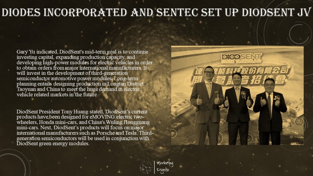
Diodes Incorporated and Sentec Set Up DiodSent JV
Diodes, a global semiconductor manufacturing supplier, partnered with Taiwanese automobile and motorcycle electromechanical system integration company Sentec to jointly hold the opening ceremony of their joint venture “DiodSent” which is expected to invest in the development of third-generation semiconductor automotive power modules and participate in the design of HEV (hybrid electric vehicles), PHEV (plug-in hybrid electric vehicles) and EV (electric vehicles).
Norway in Northern Europe and the Netherlands in Western Europe will ban the sale of traditional fuel vehicles from 2025. The major automotive powers of Germany, the United Kingdom, and Japan are expected to follow suit in 2035 which will gradually drive the penetration rate of electric vehicles. While the struggle for Taiwan’s EV market will be led by Hon Hai and Yulon joint venture “Foxtron” and the simultaneously established “MIH” platform.
Diodes Chairman, President, and CEO Keh-Shew Lu stated, Diodes and Sentec participated in six months of marathon discussions and communication to jointly establish “DiodSent.” This joint venture combines Diodes’ R&D and innovation capabilities in the field of automotive chips and Sentec’s experience in key heat dissipation materials and packaging technologies to enhance the added value of electric vehicle-related power modules and break the monopoly of major international manufacturers.
Diodes SVP Business Groups Gary Yu stated, DiodSent’s short term goal is to set up a production line with initial plans to establish a quality control system in Shanghai and other production lines in Taiwan. Annual production capacity is planned to be approximately 100,000 modules. The company’s goal is to expand production capacity to 500,000 modules within three years to enter Europe and China’s mini-vehicle power module supply chain and then prepare to win orders for electric vehicles from major international European and American manufacturers.
Gary Yu indicated, DiodSent’s mid-term goal is to continue investing capital, expanding production capacity, and developing high-power modules for electric vehicles in order to obtain orders from major international manufacturers. It will invest in the development of third-generation semiconductor automotive power modules. Long-term planning entails designing production in Longtan District, Taoyuan and China to meet the huge demand in electric vehicle related markets in the future.
DiodSent President Tony Huang stated, DiodSent’s current products have been designed for eMOVING electric two-wheelers, Honda mini-cars, and China’s Wuling Hongguang mini-cars. Next, DiodSent’s products will focus on major international manufacturers such as Porsche and Tesla. Third-generation semiconductors will be used in conjunction with DiodSent green energy modules.
Tony Huang indicated, mass production of third-generation semiconductors is scheduled to begin around the middle of next year. Therefore, in the second quarter of this year, we will begin preparing project designs including medium/low-voltage modules and high-voltage modules. Planning takes six months and mass production will be possible in the second quarter of next year at the earliest. By then, the proportion of SiC modules will reach 80%.
DiodSent VP Nai-si Hu stated, there is a serious shortage of semiconductors right now but Diodes has its own fab with a supply rate of 60% and DiodSent packaging has a supply rate of 80%. As for the third-generation semiconductors, they are developed in-house and then contracted out. Like European and US companies, DiodSent has signed long-term contracts, so there is no need to worry. There is still some time before mass production. Next, equipment will be slowly moved into the factory.
Nai-si Hu indicated, Diodes and DiodSent have utilized vertical integration to achieve a current chip output efficiency 20~30%, greater than European suppliers, so cost can be reduced by 20~30%. They are also actively participating in the MIH platform to jointly bring new automotive power semiconductors to another level. In the next two or three years, we expect to bid for orders from major international manufacturers together.
Subscribe to Power Semiconductors Weekly and watch it on YouTube every Tuesday.
If you prefer a monthly update about the world of power semiconductors delivered to your e-mail address, please, subscribe to Marketing Psycho Power Semiconductors newsletter.