Power Semiconductors Weekly Vol. 47
Deeper Integration at Higher Power
Designing state-of-the-art heat pumps and HVAC systems is not easy. Finding a way to overcome demands, such as giving more power in a smaller footprint requires a lot from a power module.
Vincotech’s new 1200V PIM+PFC is the answer. Its integrated three-phase ANPFC and inverter stage resolve contradiction to boost efficiency and cut systems costs. More compact designs at higher power ranges are not a problem any more.
Main Benefits
- All-in-one solution: 3-phase PFC with inverter stage in a compact flow1 housing allows for more compact designs and higher power density
- Highly efficient AN-PFC topology with SiC diodes for switching frequencies up to150 kHz reduces systems costs
- High speed IGBT’s in the inverter stage for high switching frequency operation
- Thin Al2O3 substrate eases the system’s thermal design
- Integrated thermal sensor simplifies temperature measurement
General Features
- Three-phase Advanced Neutral Boost PFC
- SiC components for switching frequencies up to 150 kHz
- Integrated on-board capacitors
- Kelvin emitter for improved switching performance
- Integrated sixpack with open emitter
- Built-in NTC
- Compact and low-inductive flow1 housing
Target Applications
- Embedded drives
- Heat pumps, HVAC
Alpha and Omega Semiconductor Releases 600V Low Ohmic and Fast Body Diode αMOS5™ Super Junction MOSFETs Family
Alpha and Omega Semiconductor Limited (AOS), a designer, developer, and global supplier of a broad range of power semiconductors and power ICs, and digital power products, announced the release of 600V Low Ohmic and Fast Body Diode αMOS5™ Super Junction MOSFETs Family. αMOS5 is Alpha and Omega Semiconductor latest generation of high voltage MOSFET, designed to meet the high efficiency and high-density needs for Quick Charger, Adapter, PC Power, Server, Industrial Power, Telecom, and Hyperscale Datacenter applications.
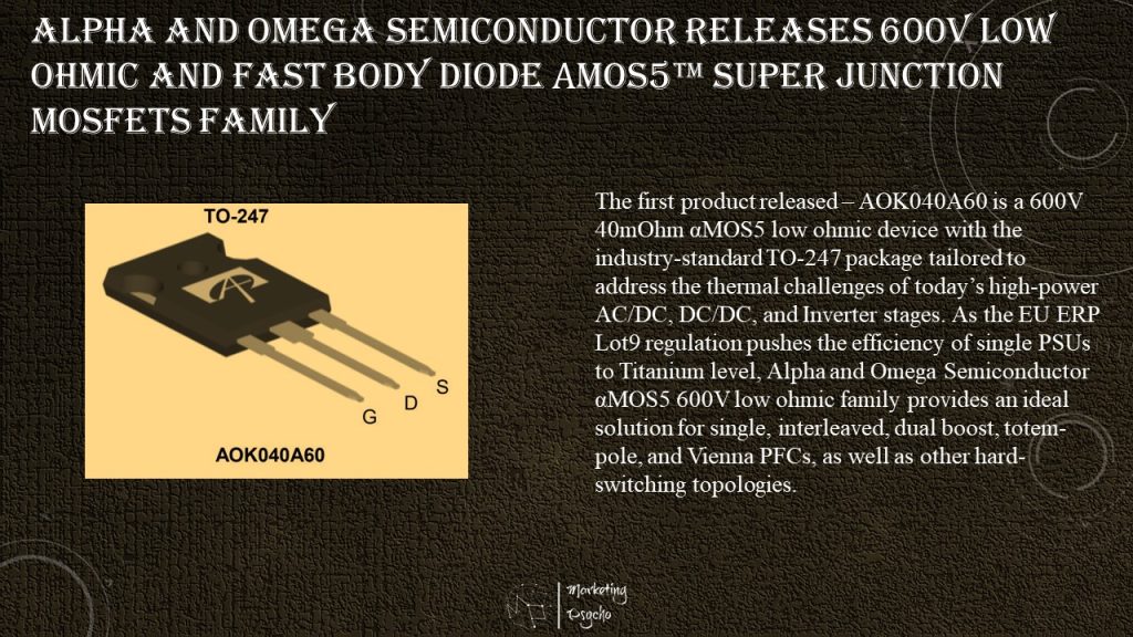
The first product released – AOK040A60 is a 600V 40mOhm αMOS5 low ohmic device with the industry-standard TO-247 package tailored to address the thermal challenges of today’s high-power AC/DC, DC/DC, and Inverter stages. As the EU ERP Lot9 regulation pushes the efficiency of single PSUs to Titanium level, Alpha and Omega Semiconductor αMOS5 600V low ohmic family provides an ideal solution for single, interleaved, dual boost, totem-pole, and Vienna PFCs, as well as other hard-switching topologies.
The 40mOhm product, followed by the upcoming 31mOhm, 65mOhm, and 80mOhm products, will provide customers with multiple choices to deal with different power ratings and efficiency requirements. The optimized capacitance of AOK040A60 will provide customers the best hard and soft switching performances, with fast turn-on/turn-off behaviors while avoiding the risks of self-turn-on or shoot-through, thanks to Alpha and Omega Semiconductor silicon design and process know-how.
The second product released – AOK042A60FD is a 600V 42mOhm FRD (Fast Body Diode) device, designed to handle the repetitive hard commutation scenario, where the MOSFET’s freewheeling body diode is reversely recovered in HB (half-bridge) or FB (full bridge) topologies. The αMOS5 600V FRD solution will further increase the system reliability as the right-fit solution for HB/FB topologies where hard switching happens during abnormal operations, such as short-circuit or start-up transients. The low Qrr of AOK042A60FD will help significantly reduce the losses during reverse recovery.
Besides Server and Telecom power supplies, the AOK040A60, AOK042A60FD and their derivatives will also target the demanding EV DC charging and Solar Inverter applications.
The 600V αMOS5 family will have a portfolio expansion including more low ohmic and FRD products coming Q1’2022. As with most of our αMOS5 products, these new devices will also be fabricated in 300mm facilities, providing better supply elasticity during the global power semiconductor shortage.
“Alpha and Omega Semiconductor’s commitment to high power SMPS applications is getting stronger. αMOS5 600V low ohmic and FRD solutions will make it possible for Server Power and Solar inverter designs to achieve higher power ratings while keeping the same form factors. Our devices’ superior efficiency will reduce customers’ TCO (total cost of ownership) by minimizing electricity, cooling and ventilation bills. Additionally, today’s EV charging stations have reached more than 50kW per module.
As power density becomes an increasingly critical differentiation factor, lower ohmic devices provide better conduction loss, thus lower thermal stress to the system. With the release of our 600V low ohmic and FRD family, we will offer the industry’s best granularity of Rdsons and packages, covering a wide range of power ratings and densities. Alpha and Omega Semiconductor market-proven αMOS5 600V low ohmic and FRD products are our answers for tomorrow’s server, telecom, solar, and EV charging applications, satisfying our customers’ growing demand for performance and reliability,” said Richard Zhang, Director of High Voltage MOSFET Product Line at Alpha and Omega Semiconductor.
Technical Highlights
- Low Ohmic devices with ultra-low switching losses
- Robust UIS under different inductive loads
- Rugged Body Diode and FRD options (Low Qrr) available for more demanding use cases
- Optimized for High Power SMPS, Solar Inverter, and EV Charging applications
Vitesco Technologies Enters into Strategic Partnership with GaN Systems Alongside a Minority Investment
Vitesco Technologies, a leading international provider of modern powertrain technologies and solutions for electric mobility, has entered into a strategic partnership with Canada based GaN Systems Inc. GaN Systems is a respected leading developer of Gallium Nitride power transistors and delivers its products amongst others to the automotive industry. GaN transistors have great potential for automotive applications because they are more efficient, smaller and in system context more economical than silicon transistors.
Particularly beneficial automotive applications are the charging and electric energy conversion in electrified vehicles. Currently, GaN-based transistors are still new for automotive use but with the joint development by GaN Systems and Vitesco Technologies, highly attractive automotive applications will become available. Power electronics based on GaN technology will help to increase vehicle range and to further improve the total energy efficiency of an electric vehicle.
Jim Witham, CEO of GaN Systems comments on the closing of the partnership: “GaN transistors are the power system technology of the future. The material enables smaller, more efficient and lower-cost power electronics. For us, it is an excellent opportunity to address the global automotive market by teaming up with Vitesco Technologies.”
Power electronics and power conversion (from AC to DC and from DC to DC) have a great influence on the energy efficiency of an electrified vehicle. During each conversion of electric energy, a certain amount of electricity is inevitably lost as heat due to the principles of physics. This impacts the total efficiency of an electric drive train. Innovative, so-called wide bandgap semiconductor materials like GaN and Silicon Carbide (SiC) offer a solution: They facilitate much higher switching frequencies, they have lower heat losses, which makes their integration into compact products easier and more cost-efficient. Vitesco Technologies is therefore already offering SiC chips in its highly efficient new traction inverter platform (EPF4). Now GaN chips are being added to the technology portfolio.
“GaN transistors help to minimize heat losses, particularly the switching losses at the high switching frequencies we require. GaN components simply outperform silicon chips in every respect. So, our early access to this pivotal technology is valuable”, explains Dr. Gerd Rösel, head of Innovation in the Electrification Technology business unit of Vitesco Technologies.
It will require qualified and specific joint development work to make GaN technology usable in the car. The return on this development work, however, is massive: Due to the efficiency of GaN transistors, as well as the resulting low cooling requirements and compact dimensions, future power electronics will be able to increase an electric car’s efficiency and range. “Together with GaN Systems we will be able to develop a platform for even more efficient automotive-grade solutions for 400 V to 800 V DC/DC conversion, for onboard chargers and in the future also for inverters”, says Rösel.
Soitec Acquires NOVASiC and Announces Strategic Partnership with Mersen to Develop New Silicon Carbide Substrates
Soitec, a world leader in designing and manufacturing innovative semiconductor materials, acquires NOVASiC, an advanced technology company specialized in polishing and reclaiming wafers on silicon carbide (SiC). The acquisition allows Soitec to drive the development of semiconductors for power supply systems in electromobility and industrial applications. The closing of the transaction is expected before the end of calendar year 2021.
In a strategic move to address the need of the automotive and industrial markets for performance and energy efficiency, Soitec is expanding its product portfolio beyond Silicon on Insulator (SOI) with silicon carbide. This crystal material unlocks greater performance, optimized design and lower environmental impact for power electronics, making it a perfect fit in particular for electric vehicles and other power efficient applications.
SmartSiC™ substrates, resulting from the application of Soitec’s unique and patented proprietary technology SmartCut™ to SiC, will enable new levels of performance and energy efficiency compared to traditional bulk silicon carbide, through higher donor wafer re-usability, improved yields and lower die sizes. In addition to reducing silicon carbide’s environmental impact in its production process, SmartSiC™ will be a catalyst to accelerate the adoption of electric vehicles. SmartSiC™ is currently at the prototyping level for devices with several key partners.
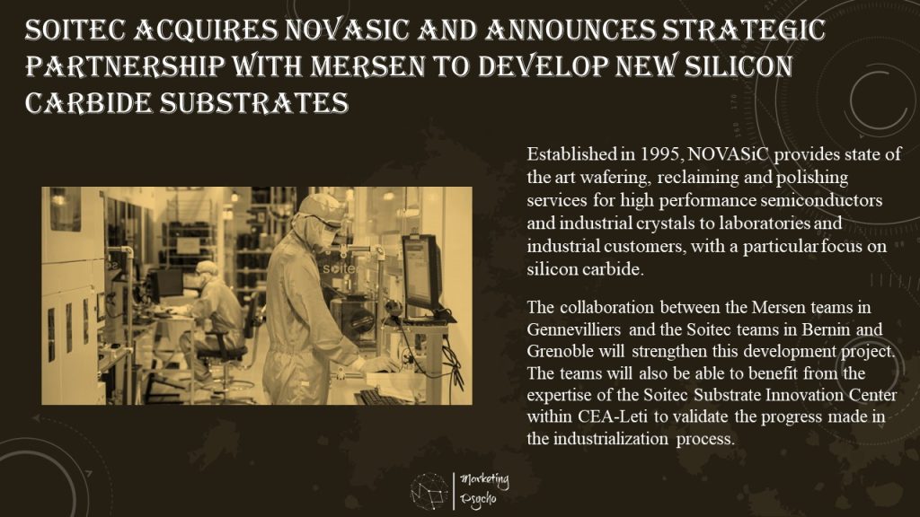
Established in 1995, NOVASiC provides state of the art wafering, reclaiming and polishing services for high performance semiconductors and industrial crystals to laboratories and industrial customers, with a particular focus on silicon carbide. The company has developed innovative polishing processes allowing enhanced device performance with a scratch free, low roughness, ultra-clean epiready surface, and no damaged layers.
With the acquisition, Didier Marsan, CEO of NOVASiC and international expert will become senior technical advisor for Soitec.
“Soitec’s SmartSiC™ substrates will be the backbone of energy-efficient electromobility,” said Bernard Aspar, COO of Soitec. “The acquisition of NOVASiC and the integration of its expertise in wafering, polishing and reclaiming brings the latest technology building block for Soitec to deliver an optimal final product and prepare the industrialization phase of our SmartSiC™ product line. The expertise of NOVASiC will help us further accelerate the go-to-market and adoption of our smart silicon carbide applications in the promising and demanding automotive and industrial markets.”
“We are very pleased to join a world-leader in semiconductor materials like Soitec,” said Didier Marsan, CEO of NOVASiC. “We look forward to providing our expertise to support the roadmap of Soitec’s new, very promising product line, and to contributing to the adoption of Soitec´s smart silicon carbide solutions.”
Besides, Soitec and Mersen, a global expert in electrical specialties and advanced materials, announced that they have entered into a strategic technical partnership to develop a new family of polycrystalline silicon carbide (poly-SiC) substrates for the electric vehicle market.
Thanks to their respective experience in substrates and materials, the joint development by Soitec and Mersen of very low electrical resistivity poly-SiC substrates will optimize SiC power electronics components devised based on Soitec’s SmartSiC™ technology. The collaboration between the Mersen teams in Gennevilliers and the Soitec teams in Bernin and Grenoble will strengthen this development project. The teams will also be able to benefit from the expertise of the Soitec Substrate Innovation Center within CEA-Leti to validate the progress made in the industrialization process.
Christophe Maleville, Soitec’s Chief Technology Officer, said: “By further pooling our materials and semiconductor expertise, we are able to produce substrates with very advanced performance. The results are compatible with our SmartSiC™ technology, and also exceed the specifications of our customers, which are the SiC power electronic circuit foundries. With its very low electrical resistivity, the poly-SiC substrate becomes a key element of our technology, and can vastly improve energy efficiency, thus making electric vehicles more efficient.”
Luc Themelin, CEO of Mersen, said: “This partnership demonstrates Mersen’s polycrystalline SiC expertise and our ability to develop a custom-design product compatible with Soitec’s technology. Thanks to this strengthened partnership, we will be able to offer the electronics industry a high-performance, cost-effective substrate for the production of power semiconductors, especially for the electric vehicle market.”
A*STAR’s Institute of Microelectronics and STMicroelectronics Team Up on SiC R&D for the EV Market and Industrial Applications
The Institute of Microelectronics (IME) at the Agency for Science, Technology and Research (A*STAR) and STMicroelectronics, a global semiconductor leader serving customers across the spectrum of electronics applications, announced the start of a Research & Development (R&D) collaboration in the field of silicon carbide (SiC) for power-electronics applications in the automotive and industrial markets. The collaboration sets a foundation for a comprehensive SiC ecosystem in Singapore and creates opportunities for other companies to engage with IME and ST in SiC research.
SiC solutions can outperform conventional silicon (Si) devices in power electronics for Electric Vehicles (EVs) and industrial applications to meet the need for power modules with smaller form factors or higher power outputs, as well as higher temperature operation. Under this research collaboration, A*STAR’s IME and STMicroelectronics aim to develop and optimize SiC integrated devices and package modules to offer significantly better performance in next-generation power electronics.
“We are pleased to collaborate with STMicroelectronics to develop breakthrough technologies that meet the needs of the growing electric vehicles market. Such efforts will continue to anchor high-value R&D activities in Singapore and bolster its reputation as an attractive regional hub for research, innovation and enterprise,” said Prof Dim-Lee Kwong, Executive Director of IME.
“This new collaboration with IME encourages the growth of a silicon carbide ecosystem in Singapore, as we ramp up our manufacturing activities there in addition to Catania (Italy). The multi-year collaborative effort helps us scale up our global R&D effort across our existing programs managed out of Catania and Norrköping (Sweden), covering the entire SiC value chain,” said Edoardo Merli, Power Transistor Macro-Division General Manager and Group Vice President of STMicroelectronics Automotive and Discrete Group. “IME’s strong knowledge and expertise in wide bandgap materials, and notably SiC, supports us in accelerating the development of new technologies and products addressing the challenges of sustainable mobility and better energy efficiency in a wide spectrum of applications.”
BorgWarner Suzhou Celebrates Phase II Ground Breaking, Enhancing R&D and Production Capabilities
BorgWarner recently broke ground on the highly anticipated second phase of its facility in the Suzhou Industrial Park and celebrated the milestone with a groundbreaking ceremony. The expansion will total 22,474 square meters and feature a four-story Research and Development (R&D) Center that will accommodate approximately 450 people as well as a two-story production workshop. All new buildings will meet the LEED Gold Standards for energy savings, emissions reduction and environmental protection, satisfying carbon peaking and neutrality goals.
“As part of our Charging Forward initiative, BorgWarner is committed to accelerating our electrification strategy and achieving carbon neutrality by 2035, with plans to grow electric vehicle product revenues to approximately 45% by 2030,” said Tom Tan, Vice President of BorgWarner Inc. and President of BorgWarner China. “Phase II of our Suzhou facility is an important milestone in BorgWarner’s China strategy. It will enhance our R&D capabilities, give us deeper market insights, and increase the manufacturing of power electronics and electronic control modules for new energy vehicles to accelerate growth in China.”
The Suzhou production site will reach an annual production capacity of 1.8 million inverters in conjunction with the development of local Viper module (Si IGBT and SiC MOSFET) fabrication, making Suzhou BorgWarner’s second largest global Viper production site. The site’s level of automation will achieve over 90%, while equipment is 100% connected with the network. The planning and scheduling, production operations, equipment management, warehousing and energy management will be digitized, creating a fully transparent and smart space. Start of production at the new buildings is expected in mid-2023.
The R&D Center of BorgWarner’s Suzhou facility will focus on the full range of electronic design and development, including power electronics, inverters and DC/DC converters, with the aim of leading power electronics technology in the Chinese market. In the coming years, BorgWarner Suzhou will expand the R&D team, establishing full design capabilities, and equip the center with additional test and prototype equipment to enable the team to serve its customers more quickly and efficiently.
“Upon completion of the second phase of the Suzhou facility, we will be able to provide our customers with premium quality NEV motor controllers, while enhancing our local capabilities in prototyping and testing of electronic control products,” said Dr. Shawn Li, Vice President and General Manager Asia, BorgWarner PowerDrive systems. “Our Suzhou facility will have the capacity to produce 13 million Viper products and over 1.8 million inverter products per year, accelerating our rapid growth in the Chinese market.”
The groundbreaking ceremony brought together local government representatives, customers including Volvo, Great Wall Motor, Changan, BYD, Li Auto, XPeng Motors, ZEEKR and Cummins, suppliers, and media who commemorated the grand occasion with BorgWarner’s management and employees to celebrate the launch of Phase II of BorgWarner’s Suzhou Facility.
WeEn Technology Answers the Call for Higher Efficiency
The power we use to run electrical appliances, satiate our growing obsession with generating, processing and consuming data, and support mobility for work and pleasure comes at the cost of a trade-off with the habitable environment. As the effects of this unwelcome exchange become increasingly immediate, government and industry alike are responding with regulations and standards aimed at reigning in energy consumption and shifting toward renewable energy sources.
While individually each of the applications like HVAC, datacenter servers, solar and wind power storage, and electric vehicle (EV) fast chargers and traction inverters, have specific design requirements, the common trends of high efficiency, high power density, and lower cooling requirements are dominant for them all.
For instance, datacenters are estimated by the International Energy Agency (IEA) to have consumed anywhere between 200 TWh and 250 TWh in 2020 or about one percent of the global electricity demand. As the global internet traffic shot up by over 40% last year with expectations of continued growth, the U.S. is using the Energy Act (2020) to formalize a government-industry joint effort to increase energy efficiency at federal government datacenters and, eventually, across the industry. In Europe, major datacenter operators have signed the Climate Neutral Data Centre Pact to achieve climate neutrality by 2030. And these efforts are supported by high efficiency requirements of about 96% at half-load and about 91% at full-load from Energy Star’s 80 Plus Titanium certification as well as Ecodesign in Europe (ErP) Lot 9 regulation.
In the range-anxious EV market, efficiency is a synonym for success. Fast charging is another, as it reduces the time spent at the charging station. Car makers are therefore moving toward the 800 V EV bus, which enables them to deliver higher power to the battery without increasing current and, therefore, without increasing the size and weight of copper used in EVs.
In the renewable energy market, where solar panels themselves are not known for efficiency, lower loss in the power electronics is equally precious.
Power density without significant trade-off toward cumbersome cooling systems is important to datacenters, solar power plants and EV charging stations not only because space costs but because smaller, lighter systems are easier, faster and cheaper to install.
This tall order for converters, inverters and all types of power supplies means that they should be able to:
- Switch at high frequency in order to decrease the size, weight and cost of the inductors.
- Have low losses to improve both system efficiency and lower the size, weight and cost of the cooling requirement.
- Be able to tolerate higher temperatures without sacrificing overall power density to cooling requirements.
- Support higher power/voltages needed to reduce system I2R losses.
Where silicon (Si) fails to achieve the specifications needed, silicon carbide (SiC)-based components, such as Schottky diodes and MOSFETs, enable applications with a significantly lower energy impact. This is because SiC is a wide bandgap semiconductor that has:
- A much lower ON-state voltage drop, which reduces conduction losses, and lower OFF-state leakage currents than Si.
- Higher edge rates during switching, thus lower switching losses.
- Higher breakdown field that allows higher voltages and a much higher thermal conductivity that allows devices to cool faster.
- Robustness against temperature, thus lowering cooling requirements.
This is the reason the use of SiC diodes and MOSFETs in power electronics is growing rapidly. Market research firm Omdia expects the wide bandgap (GaN and SiC) discrete market share to increase from 5% in 2020 to 17% in 2024, growing at nearly 4.4% CAGR.
Although we use SiC Schottky diodes in power applications for a couple of decades, the device design and manufacturing technology have continued to evolve and contribute to this growth. For instance, the U.S. Department of Energy’s Solar Energy Technologies Office (SETO) has a funding program to examine issues related to efficiencies in generating, distributing and storing solar energy. It counts as participants both companies developing SiC-based high-voltage converters and string inverters, as well as university research teams working on SiC technologies.
In the EV area, Yole Développement estimates power SiC devices in EV/HEV will grow beyond $1.5 billion in 2025 at a CAGR during 2019-2025 of 29 percent. We use SiC in several EV systems, including the traction inverter, the DC-DC converter, the on-board charger, as well as fast-charging (off-board) infrastructure that tackles the last barrier to widespread EV acceptance.
WeEn Semiconductors addresses this market demand for SiC components with SiC Schottky diodes. The company has a 50-year history in power-device development and manufacturing, starting as an effort by Philips, then NXP before being spun off as WeEn Semiconductors in 2015 armed with a merged PiN Schottky (MPS) technology for manufacturing SiC Schottky diodes.
Based in China, the company now has a global footprint comprising two R&D centers, two application laboratories, one reliability and failure analysis laboratory, 10 WeEn corporate entities, 12 sales offices, and six representative offices together employing 350 staff worldwide.
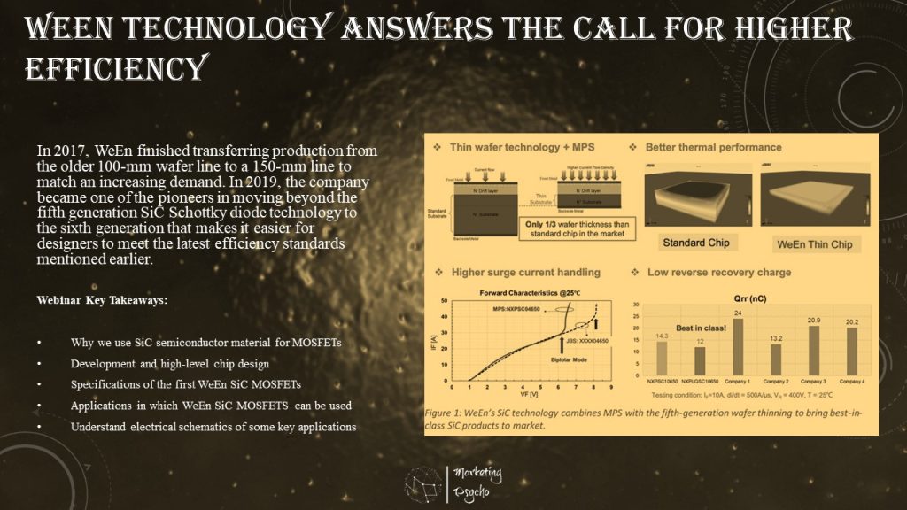
In 2017, WeEn finished transferring production from the older 100-mm wafer line to a 150-mm line to match an increasing demand. In 2019, the company became one of the pioneers in moving beyond the fifth generation SiC Schottky diode technology to the sixth generation that makes it easier for designers to meet the latest efficiency standards mentioned earlier.
The MPS technology builds on the Junction Barrier Schottky (JBS) concept that uses P islands in the N- epitaxial layer to move the peak in the reverse-mode electric field away from the Schottky layer, thereby reducing reverse leakage current and attendant losses. An MPS diode introduces relatively larger P+ regions in the N- epitaxial layer connected through ohmic contacts.
This combines the low forward voltage advantage typical of the SiC Schottky diode with the better inrush current handling of the PiN diode. At high forward current density or a surge, the PN junction in the MPS structure injects minority carriers in the drift region of the diode thereby lowering the forward voltage drop at high current density.
Increasing the PN area means reducing the Schottky area, which increases ON-resistance at nominal forward current. WeEn addresses this by using proprietary low-resistance ohmic contacts to the P+ region to reduce the overall ON-resistance. WeEn SiC MPS diodes thus have better surge current handling than competing parts without trading off current conduction capability.
The company has further developed device technology, reducing the N+ substrate thickness by “back-grinding” such that the resulting wafer thickness is only one-third that of standard chips on the market. The wafer thinning significantly reduces the contribution of the substrate to the total ON resistance. It also results in a much lower thermal resistance so that a lowering of junction temperature by as much as 50°C is achieved.
WeEn SiC parts are also best-in-class in terms of the reverse recovery charge, Qrr. The temperature-independent low Qrr allows designers to use WeEn Schottky parts in high-frequency switching applications, such as power factor correction (PFC) circuits that can switch up to 140 kHz. Moreover, the parts are qualified up to junction temperatures of 175°C.
These characteristics address the previously discussed high efficiency and power density, and low cooling requirements from applications today.
WeEn’s older generation offerings are comparable to fifth-generation products in the mainstream market but with better surge current handling. Their latest G6 products with ultra-low VF are comparable to competing Gen.6 products but with significantly lower junction-to-case thermal resistance and therefore higher current handling capability.
The compelling benefits of SiC devices has increased their adoption with EV on-board charger and traction, as well as charging infrastructure markets expected to grow rapidly. Yole Développement expects the automotive segment to capture as much as 60 percent of the SiC market share in 2026.
WeEn therefore continues to develop not only its SiC technology and but higher-performance packages. Its recently launched automotive qualified (AECQ-101) is a testament to future product development focus. The company is working to expand its 650-V and 1200-V Schottky diode portfolio to 1700 V and has planned 1200-V MOSFETs as well as MOSFET modules in its technology roadmap.
Besides, WeEn Semiconductors is introducing its first SiC MOSFETs, complementing the SiC Diodes that are already in the WeEn portfolio. The SiC MOSFETs can be used in very fast switching PFC (power factor correction) circuits and LLC converters in for instance UPS, SMPS and EV Chargers. SiC enables high switching frequencies, resulting in smaller and lower cost passives and higher efficiency of the power conversion.
Join this WeEn Semiconductors ‘Introduction to Silicon Carbide SiC MOSFETs: Design, Products, Applications’ webinar on December 09, 2021, to learn more about SiC MOSFETs.
Key Takeaways:
- Why we use SiC semiconductor material for MOSFETs
- Development and high-level chip design
- Specifications of the first WeEn SiC MOSFETs
- Applications in which WeEn SiC MOSFETS can be used
- Understand the (simplified) electrical schematics of some key applications
- Date: December 09, 2021
- Time: 10 AM CET
- Duration: 1 hour
Subscribe to Power Semiconductors Weekly and watch it on YouTube every Tuesday.
If you prefer a monthly update about the world of power semiconductors delivered to your e-mail address, please, subscribe to Marketing Psycho Power Semiconductors newsletter.