Power Semiconductors Weekly Vol. 34
Infineon and Panasonic Accelerate GaN Technology Development for 650 V GaN Power Devices
Infineon Technologies AG and Panasonic Corporation have signed an agreement for the joint development and production of the second generation (Gen2) of their proven gallium nitride (GaN) technology, offering higher efficiency and power density levels. The outstanding performance and reliability combined with the capability of 8-inch GaN-on-Si wafer production mark Infineon’s strategic outreach to the growing demand for GaN power semiconductors.
In accordance with market requirements, Gen2 will be developed as 650 V GaN HEMT. The devices will allow for ease of use and provide an improved price-performance ratio, targeting, amongst others, high- and low-power SMPS applications, renewables, motor drive applications.
For many designs, gallium nitride (GaN) offers fundamental advantages over silicon. The outstanding specific dynamic on-state resistance and smaller capacitances compared to silicon MOSFETs qualify GaN HEMTs for high-speed switching. The resulting power savings and total system cost reduction, operation at higher frequencies, improved power density, and overall system efficiency make GaN a very attractive choice for design engineers.
“In addition to the same high reliability standards as for Gen 1, with the next generation customers will benefit from even easier control of the transistor as well as a significantly improved cost position, thanks to moving to an 8-inch wafer manufacturing,” says Andreas Urschitz, President of Infineon’s Power and Sensor Systems Division. Like the jointly developed Gen 1 devices, known as Infineon’s CoolGaN™ and Panasonic’s X-GaN™, the second generation will be based on the normally-off GaN-on-silicon transistor structure. This, in combination with the unmatched robustness of the hybrid-drain-embedded gate injection transistor (HD-GIT) structure, makes these components the product of choice and one of the most long-term reliable solutions in the market.
“We are delighted to extend our partnership and collaboration with Infineon on GaN components. Within the joint approach, we will be able to apply Gen1 and Gen2 devices on high quality and based on latest innovation developments”, says Tetsuzo Ueda, Associate Director of Engineering Division, Industrial Solutions Company, Panasonic Corporation.
The market launch of the new 650 V GaN Gen2 devices is planned for the first half of 2023.
SMIC to Build $8.87bn Shanghai Chip Plant in Challenge to TSMC
China’s top chipmaker SMIC will build a nearly $9 billion chip plant in Shanghai, challenging global leader Taiwan Semiconductor Manufacturing Co. amid an industrywide rush to expand capacity.
The plant will be Semiconductor Manufacturing International Corp.’s (SMIC) biggest investment in years and will churn out older-generation chips that are currently in short supply for everything from consumer electronics to self-driving cars.
SMIC said in a stock exchange filing that it has agreed with the Lin-gang Special Area of China (Shanghai) Pilot Free Trade Zone to form a joint venture to build and operate the plant. Capacity is planned to reach 100,000 wafers a month, with a total investment of $8.87 billion.
The plant will make chips using 28-nanometer production tech or older, which is suitable for such chips as image sensors, Wi-Fi chips, driver ICs and microcontrollers, many of which are in extremely short supply. The most advanced chips on the market are made using 5-nm technology for iPhone processors and Mac CPUs.
TSMC, the world’s biggest contract chipmaker, announced a similar move this year, saying it will spend $2.8 billion to expand its production capacity in the Chinese city of Nanjing for 28-nm tech to tap growing local demand. Other global peers, including Globalfoundries and United Microelectronics, are also aggressively expanding capacity.
The registered capital of SMIC’s joint venture will be $5.5 billion, according to the filing, with the chipmaker taking at least a 51% stake and shouldering responsibility for its operations and manufacturing. The Shanghai government will take a 25% stake and third-party investors will be sought for the remainder, the filing said. It was not immediately clear when the new facility is slated to begin production
SMIC announced this year that it will jointly invest in a $2.35 billion chip project with the Shenzhen government to churn out 40,000 wafers a month in the southern Chinese city, starting in 2022.
Last September, SMIC was added to the U.S. Commerce Department’s Entity List, which bans the unlicensed exports of American technology to the company.
SMIC co-CEO Zhao Haijun has confirmed several times that the U.S. blacklisting has hindered the company’s development of more advanced technologies, which rely more heavily on American equipment suppliers such as Applied Materials and Lam Research. Zhao said his company is looking for alternative solutions while continuing to communicate with the U.S. government.
SMIC is China’s most promising contract chipmaker and thus shoulders many of Beijing’s hopes for building a self-reliant chip industry.
Recently the company has benefited from a surge in prices for chipmaking services as global electronics manufacturers and automakers battle an unprecedented shortage of semiconductors. SMIC is a key production partner for many Chinese chip developers, as well as U.S. chip developer Qualcomm. The company reported record earnings for the first half of 2021, thanks to higher prices and robust demand.
5-year Plan Gives Leg Up to Chip Base Material
China’s top industry regulator will include silicon carbide, or SiC, an important semiconductor base material, into a five-year plan for industrial technological innovation development.
The move is part of broader efforts by the Ministry of Industry and Information Technology to guide development of carbon-based materials to support chip innovation and development, experts said.
Carbon-based materials can be good substitutes for silicon-based semiconductor materials, and they form an important part of the third-generation semiconductor technologies where China aims to achieve breakthroughs, experts said.
The Ministry of Industry and Information Technology said it will include carbon-based materials in the 14th five-year plan (2021-25) for raw material industrial development, and also include SiC and carbon matrix composites in the 14th five-year plan for industrial technological innovation development. The larger goal is to support the industry to tackle technology barriers, so as to improve product quality and promote modernization of industry chains.
Dongxing Securities said in a research note that silicon, which is found in large natural reserves, has become the most important raw material for the manufacture of chips and devices. More than 90 percent of semiconductor products are made of silicon as a substrate.
But limited by the characteristics of the material itself, silicon-based power devices are gradually unable to meet the requirements for high-power and high-frequency devices in emerging applications like 5G, new energy vehicles, and high-speed rail.
So, SiC is expected to partially replace silicon and become a new substrate material for the preparation of high-voltage and high-frequency devices, Dongxing Securities said.
SiC is an important material of the third-generation semiconductor technologies, as China seeks breakthroughs in the third-generation chips for the “post-Moore Era”. In 1975, Intel co-founder Gordon Moore formulated a rule that the number of transistors on a silicon chip doubles roughly every two years. But rapid technological advancements may make the rule obsolete in the future.
In May, a government meeting attended by Vice-Premier Liu He discussed the potential disruptive technologies of integrated circuits, or ICs, in the post-Moore era.
Yuekai Securities said in a research note it is clear the third-generation semiconductor technologies are an important development direction, with their downstream applications focusing on 5G base stations, new energy charging piles, intercity high-speed rail transit and other areas.
The third-generation semiconductor technologies offer a good opportunity for Chinese chipmakers to catch up with their foreign counterparts. Third-generation semiconductor products mainly use mature manufacturing and processing technologies, where domestic manufacturers will face fewer obstacles than in the traditional silicon-based semiconductor technologies, Yuekai Securities added.
Xiang Ligang, director-general of the Information Consumption Alliance, a telecom industry association, said: “The main battlefield of the applications of third-generation semiconductor technologies is in China, but it will take a long time for domestic companies to address a string of challenges before widely popularizing these technologies.”
Hongwei Technology Power Semiconductors Company Went Public
Jiangsu Hongwei Technology Co., Ltd. was successfully listed on the Science and Technology Innovation Board. Hongwei Technology has also become another power semiconductor company that has successfully landed on the Sci-tech Innovation Board after China Resources Micro and Yinhe Microelectronics.
Hongwei Technology was established in 2006 by Jinshitong, Century Dongxu and Zhao Shanqi, with a registered capital of 20 million yuan. Its main business is power semiconductor chips and power modules based on IGBT.
According to MINNEWS in recent years, Hongwei Technology has established a relatively stable relationship with industry leaders or well-known corporate customers such as Delta Group, Inovance Technology, Jasic Technology, Aotai Group, Suzhou Goodtech, Shenghong Co., Ltd., Incore, Crestal, etc. Supporting partnership. From 2018 to 2020, Hongwei Technology’s total revenue will be 262 million yuan, 260 million yuan and 332 million yuan, respectively.
In this IPO, Hongwei Technology plans to raise 557.5 million yuan, which will be used for three projects – “New Power Semiconductor Device Industry Base”, “R&D Center Construction”, and “Repaying Bank Loans and Supplementing Working Capital”.
IGBT Market and Technology Trends 2021
An Insulated Gate Bipolar Transistor (IGBT) is a key device in numerous power electronics applications. The IGBT market was worth $5.4B in 2020 and will grow with a Compound Annual Growth Rate (CAGR) of 7.5% from 2020-2026.
Discrete IGBTs and IGBT power modules can be found in applications like electric and hybrid electric vehicles (EV/HEVs), industrial motor drives, wind turbines, photovoltaic installations, trains, Uninterruptible Power Supplies (UPS), EV charging infrastructure and home appliances. In 2020, the largest IGBT market segments were industrial applications and home appliances. They were closely followed by EV/HEVs, which represented a market of $509M in 2020 and which will grow with an impressive CAGR for 2020-2026 of 23%. This is due to the transition from Internal Combustion Engine (ICE) vehicles to EV/HEVs, which is being strongly driven by governments’ targets for CO2 emissions reductions.
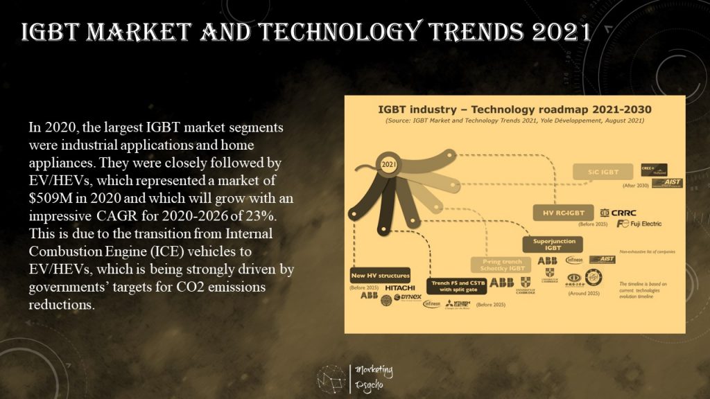
Yole Développement updated their IGBT Market & Technology Trends report. It contributes to the understanding of the overall ecosystem, its latest innovations and the strategy of leading power electronics companies. Including market trends and forecasts, supply chain, technology trends, technical insights, and market segmentations, take away and outlook. This study delivers an impressive overview of the power electronics industry with a special focus on IGBT market segment.
Heraeus Electronics at PCIM Asia 2021
The power electronics assembly market evolves at a fast pace, and competition becomes more intense. The power semiconductor industry is undergoing a technology revolution, led by Wide Band-gap (WBG) semiconductors like silicon carbide (SiC) and gallium nitride (GaN), to enable higher power densities and switching frequencies. However, these challenges and requirements cannot be met by the prevailing power electronics packaging technologies and solutions, which have become a bottleneck to achieve the best result in WBG semiconductors. Therefore, the next-generation packaging materials and matched solutions are key to the WBG-enabled transformation. With Heraeus Electronics, customers reach key targets for the development of their innovations by optimizing materials and matched materials combinations.
During PCIM Asia 2021 Heraeus Electronics will hold a presentation ‘Advanced Packaging Solutions for SiC Based EV Inverter System’ where they will show a full packaging solution for SiC power devices adopting novel packaging materials, including silver sinter materials, high reliability metal ceramic substrate and Die Top System (DTS). They will further show how and to what extent this solution can maximize the packaging performance.
- Date: 9th September 2021, 15:10 – 15:30
- Venue: Hall 11, Shenzhen World Exhibition & Convention Center
- Topic: Advanced Packaging Solutions for SiC Based EV Inverter System
- Speaker: Dr. Jing Zhang, Director of innovation China, Heraeus Electronics
Avnet Webinars: Power Solutions for Vehicles and Fast Charger Applications
Join Avnet Silica at this webinar series dedicated to vehicular and infrastructure applications (eChargers).
With sessions run by the experts from Avnet Silica partners Nexperia, onsemi, ROHM and STMicroelectronics they’ll cover the topologies, reference designs and technologies that are shaping the next generation of electric vehicles.
Transformation of the automotive market is already underway, and innovations in semiconductor technologies are now enabling the utilization of wide bandgap for applications in electrified transportation. These advancements mean that many electric vehicles, from industrial and urban cleaning machines, to farm and building, and tractors, forklifts and even boats, will be required to comply with low emission electric or hybrid design.
At this webinar, you will learn about:
- Multiple solutions for different electrical specs
- Mechanical and thermal requirements
- Solutions for efficiency, density and cost optimization
- Latest innovative solutions from Avnet Silica partners
Agenda:
- 10:00 AM CEST – Nexperia GaN FET’s for improved efficiency, stability and robustnesses in your next generation applications
- 10:35 AM CEST – onsemi Charging and driving solutions for non automotive electrical vehicle
- 11:05 AM CEST – STMicroelectronics SiC MOSFETs and galvanically isolated gate drivers, the perfect combination for high-power converters and chargers for Industrial and EV applications
- 11:35 AM CEST – ROHM Solutions for EV charging & Integrated 1700V SiC MOSFET for industrial auxiliary power supply solutions
The webinars will be held on September 14 and 17, 2021.
Subscribe to Power Semiconductors Weekly and watch it on YouTube every Tuesday.
If you prefer a monthly update about the world of power semiconductors delivered to your e-mail address, please, subscribe to Marketing Psycho Power Semiconductors newsletter.