Power Semiconductors Weekly Vol. 30
Lower Your Total Cost of Ownership with High Performance Si3N4 AMB Substrates
Silicon Nitride (Si3N4) Active Metal Brazed (AMB) substrates are becoming increasingly popular for multi-chip power modules as a tool for achieving the highest possible power densities. This is due to their excellent thermal and mechanical properties. Nevertheless, as pressures on cost and performance continue to increase alongside the growing importance of power semiconductors in applications — e.g., electric vehicles and energy storage — innovations are needed to address the evolving needs of the market. Fortunately, a new Si3N4 raw ceramic material is now available, and Rogers is leveraging its strong partner network to deliver large-scale production of higher performing Si3N4 AMB substrates.
The intrinsic material properties of Si3N4 indicate that its thermal conductivity can be more than 200 W/mK. However, multiple factors, including the raw materials’ purity and, particularly, the control of the oxygen content, the orientation of β- Si3N4 grains and the glassy phase at the grain boundaries are limiting the thermal conductivity of currently available Si3N4 raw ceramic substrates. Nowadays, typical values for commercially available products are range between 80 and 90 W/mK at room temperature.
Manufacturers of Si3N4 raw ceramic substrates are working hard to improve thermal conductivity. Research has shown that it’s possible to produce Si3N4 raw ceramic substrates with thermal conductivity up to 177 W/mK. Also, optimized process conditions have shown to improve thermal conductivity in the thickness direction as opposed to the in-plane direction. These efforts are paying off. The latest results show that a thermal conductivity in the range between 110 and 130 W/mK at room temperature is feasible, not only at lab scale but also under serial production conditions. In addition, the raw ceramic substrates´ mechanical properties remain very good with characteristic values of the bending strength in the range of 600-700 MPa.
These recent advancements open new opportunities for the design of power modules. A reduction of the thermal resistance can be achieved with the same ceramic thickness which are already used for existing power modules. Consequently, module makers can upgrade the output power of their existing modules by an easy drop-in replacement of the substrate. There would be no need to redesign the packaging, and there would be no additional tooling costs. Assembly and interconnection technologies remain unchanged, so the new solution could be brought to market in a very timely manner.
Another way to look at it is to utilize these substrates with higher thermal conductivity to achieve a reduction of chip area and hence chip cost savings. This could be interesting particularly for silicon carbide (SiC) modules because SiC devices are much more expensive than their silicon counterparts and are therefore the main cost driver for the modules. Besides, SiC technology is likely to make significant progress in the coming years. One can expect new generations of smaller chips with a lower specific on-state drain to source resistance to come to the market very soon. In this case, the higher thermal conductivity of the ceramic can compensate the smaller chip area.
Ultimately, higher power densities can be achieved without any compromise on the modules´ lifetime. The higher thermal conductivity does not only limit the increase of the chip junction temperature, but also, the superior mechanical properties are advantageous when the substrates are exposed and must resist harsh thermal cycling conditions.
As the market and technology leader for metallized ceramic substrates, Rogers has quickly identified the opportunity to unleash the commercial and technological potential of such innovative products. Rogers is now capable of delivering Si3N4 AMB substrates with improved thermal performance to its broad customer base. While the final qualification is ongoing, first samples are already available for customer evaluation. Furthermore, thermal simulations can be performed to understand the substrates potential benefits for target application.
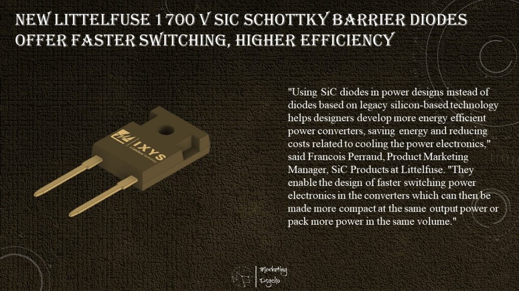
New Littelfuse 1700 V SiC Schottky Barrier Diodes Offer Faster Switching, Higher Efficiency
Littelfuse, Inc., an industrial technology manufacturing company empowering a sustainable, connected, and safer world, announced the expansion of its silicon carbide (SiC) diodes portfolio to include the 1700 V-class.
The LSIC2SD170Bxx Series SiC Schottky Diodes are available in the TO-247-2L package with a choice of current ratings (10A, 25A, or 50A). They offer power electronics system designers a variety of performance advantages, including close-to-zero reverse recovery current, high surge capability, and a maximum operating junction temperature of 175°C, so they are ideal for applications that require enhanced efficiency, reliability, and simplified thermal management.
SiC Schottky barrier diodes are ideal in a wide range of AC/DC and DC/DC power converters for industry, energy generation, and energy distribution/storage, including:
- Industrial switch-mode power supplies
- Uninterruptable power supplies
- Battery chargers
- Solar inverters
- Industrial motor drives
- High speed rectifiers
“Using SiC diodes in power designs instead of diodes based on legacy silicon-based technology helps designers develop more energy efficient power converters, saving energy and reducing costs related to cooling the power electronics,” said Francois Perraud, Product Marketing Manager, SiC Products at Littelfuse. “They enable the design of faster switching power electronics in the converters which can then be made more compact at the same output power or pack more power in the same volume.”
The LSIC2SD170Bxx SiC Schottky diodes offer these key benefits:
- Positive temperature coefficient of the forward voltage for safe operation and ease of paralleling
- Extremely fast, temperature-independent switching
- Dramatically reduced switching losses compared to Si bipolar diodes
- Optimized overall system efficiency
First Aerospace-qualified Baseless Power Module Family Improves Aircraft Electrical System Efficiency
In the race to reduce aircraft emissions, developers increasingly are moving toward more efficient designs including electrical systems that replace today’s pneumatics and hydraulics powering everything from on-board alternators to actuators and Auxiliary Power Units (APUs). To enable next-generation aircraft electrical systems, new power conversion technology is required. Microchip Technology Inc. announced its development with Clean Sky, a joint European Commission (EC) and industry consortium, of the first aerospace-qualified baseless power modules enabling higher-efficiency, lighter and more compact power conversion and motor drive systems.
Partnering with Clean Sky to support aerospace industry goals set by the EC for stricter emission standards that result in climate neutral aviation by 2050, Microchip’s BL1, BL2 and BL3 family of baseless power modules provides greater efficiency in AC-to-DC and DC-to-AC power conversion and generation through the integration of its silicon carbide power semiconductor technology. Forty-percent lighter than others due to the modified substrate, the innovative design also produces an approximate 10% cost savings over standard power modules that incorporate metal baseplates. Microchip’s BL1, BL2, and BL3 devices meet all mechanical and environmental compliance guidelines set forth in RTCA DO-160G, the “Environmental Conditions and Test Procedures for Airborne Equipment,” Version G (August 2010). RTCA is the industry consortium that develops consensus on critical aviation modernization issues.
The modules are available in low-profile, low-inductance packaging with power and signal connectors that designers can solder directly on printed circuit boards, helping to speed development and increase reliability. And, the same height between the modules in the family enables them to be paralleled or connected in a three-phase bridge and other topologies to achieve higher-performing power converters and inverters.
”Microchip’s powerful new modules will help to drive innovation in aircraft electrification and, ultimately, progress toward a future of lower emissions,” said Leon Gross, vice president of Microchip’s discrete products business unit. “This is an enabling technology for the systems ushering in a new era of flight.”
The family incorporates silicon carbide MOSFETs and Schottky Barrier Diodes (SBDs) to maximize system efficiency. In packages delivering 100W to more than 10 KW of power, the BL1, BL2, and BL3 family is available in numerous topology options including phase leg, full bridge, asymmetric bridge, boost, buck and dual common source. These high-reliability power modules are available in voltage ranges from 600V to 1200V in silicon carbide MOSFETs and IGBTs to 1600V for rectifier diodes.
Microchip’s power module technology as well as its ISO 9000- and AS9100-certified fabrication facilities provide high-quality units through flexible manufacturing alternatives.
While introducing new innovations the company also teams with system manufacturers and integrators on obsolescence management, supporting customers’ efforts to minimize redesign work and lengthen life cycles, thereby reducing overall system costs.
The company’s baseless power modules complement its aerospace portfolio of motor drive controllers, storage integrated circuits, Field Programmable Gate Arrays (FPGAs), microcontrollers (MCUs), microprocessors (MPUs), timing products, semiconductors and point-of-load regulators – providing designers with total system solutions for a wide variety of aerospace and defense applications. Microchip also provides a full portfolio of silicon carbide technology solutions for aerospace, automotive and industrial applications.
Driving Electromobility and Energy Efficiency Forward: Infineon on Board the VW ID.4 USA Tour
Electromobility is fast becoming a reality. In fact, every seventh car produced today is operating on a form of electrification. Demonstrating the power and convenience of an electric vehicle (EV), Volkswagen of America has teamed up with long-distance driving expert Rainer Zietlow for the VW ID.4 USA tour that recently kicked off at Volkswagen of America’s headquarters in Herndon, VA. Infineon Technologies AG, a world leader in semiconductors for mobility, energy efficiency and the IoT, is on board of the new VW ID.4 with over 50 semiconductors and enabling energy efficient electric drives and charging infrastructure. Moreover, the drive route of the tour, which will be crisscrossing the United States, will incorporate five Infineon facilities including Livonia, MI; San Jose, CA; Austin, TX; El Segundo, CA; and Washington D.C.
“Infineon supports climate protection through reduction of our own carbon emissions, along with products and technologies that enable renewable power generation, efficient storage, and sustainable mobility,” said Lars Ullrich, Vice President of Automotive, Infineon Technologies Americas. “Our semiconductors are at the heart of vehicle electrification and the enabling charging infrastructure. By increasing range, efficiency and accessibility, we are helping the automotive industry to successfully achieve the fundamental transformation towards electromobility – to protect the environment without compromising drivers’ flexibility and comfort.”
Stringent CO2 emission standards are accelerating EV adoption globally. In the U.S., for example, the state of California mandates that by 2035, all new cars and passenger trucks sold must be zero-emission vehicles. Changing consumer preferences and the availability of new EV models have further increased EV adoption over the last year.
Semiconductors play a major role for electromobility by powering electric drives and laying the foundation for carbon-neutral mobility of the future. Well above 50 percent of all vehicles newly produced at the end of this decade are expected to be driven by a partially or fully electric powertrain. Guided by the principles of ‘clean, safe and smart,’ Infineon is working with car manufacturers and suppliers to create vehicles with electric drivetrains and provides a multitude of semiconductor solutions. Already this year, over 35 electric and plug-in hybrid models with a drivetrain incorporating power semiconductors from Infineon will be in production worldwide.
The ID.4 is Volkswagen’s first all-electric SUV and the brand’s first global EV. At launch in the U.S., it is powered by a 77 kWh (net) battery pack and has a range of approximately 517 kilometers (WLTP) in ID.4 Pro rear-wheel-drive models. At a public DC fast-charging station, with 125 kW charging, the ID.4 can go from five to 80 percent charged in about 38 minutes. Infineon provides over 50 semiconductor components for the ID.4, including power semiconductors, microcontrollers and driver ICs. At the heart of the electric drivetrain is a power module from the HybridPACK™ Drive product family for the conversion of energy between the battery and motor. Looking beyond the car, semiconductors from Infineon are also playing an important role in the electric charging infrastructure and enabling faster charging.
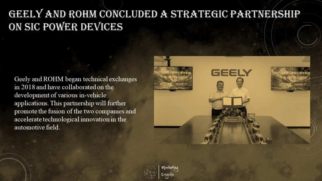
Geely and ROHM Concluded a Strategic Partnership on SiC Power Devices
Geely Automobile Company (Geely), a leading Chinese automobile manufacturer, and ROHM Co., Ltd. (ROHM), a global semiconductor manufacturer, are strategically involved in an advanced technological development in the automobile field.
Geely and ROHM began technical exchanges in 2018 and have collaborated on the development of various in-vehicle applications. This partnership will further promote the fusion of the two companies and accelerate technological innovation in the automotive field.
Geely leverages ROHM’s advanced power solutions centered on SiC power devices to develop highly efficient traction inverters and in-vehicle charging systems to extend the range of electric vehicles, reduce battery costs, and charge time.
As the first result, a traction inverter equipped with ROHM’s SiC power device was adopted for the platform for electric vehicles currently under development by Geely.
Through this partnership, Geely and ROHM will promote the development of low-carbon technologies in the automobile industry and the technologies that realize a safe and secure mobility society, and contribute to the realization of a sustainable society.
Space Industry Launches with GaN Systems
The space race is heating up, with Richard Branson’s Virgin Galactic and Jeff Bezos’ Blue Origin having recently launched their first space flights. While these “New Space” companies are making headlines, “Old Space” organizations such as government agencies and large, traditional aerospace companies continue to push the boundaries of outer space. All space-related transport and instruments require highly reliable (HiRel) power solutions designed specifically to withstand the harsh environments necessary for space applications.
GaN-powered systems revolutionize capabilities in propulsion systems to meet challenges in high power, high density motors; avionics systems and subsystem point-of-load converters; and aerospace power and energy storage for power conversion and control, distribution, and transmission. GaN Systems power transistors deliver the efficiency, size, and power-density benefits required for demanding HiRel power applications.
NASA is developing Europa Clipper, an interplanetary mission to conduct detailed reconnaissance of Jupiter’s moon Europa and investigate whether it can harbor conditions suitable for life. For this mission, NASA’s Jet Propulsion Laboratory (JPL) will need various instruments to collect and measure critical data while the spacecraft is in orbit. The organization has shifted away from silicon toward GaN technology for the essential components that power these activities, due partly to the reduced cost-per-pound enabled by GaN. GaN Systems’ transistors have delivered impressive results for NASA, and will be used for the Europa Clipper project. “It’s very expensive to send massive objects in orbit or fly flight hardware,” said Peter Majewicz, NEPP program manager. “We’re always looking for ways to bend the ratio to be more advantageous in order to reduce size or weight or increase power for more benefit, and that’s something GaN offers.”
“New Space” companies are also busy introducing new solutions to explore the wild space frontier. In 2021 alone, Virgin Galactic launched the VSS Unity SpaceShip Two vehicle, Blue Origin launched the New Shepard rocket ship, and SpaceX is launching the Transporter-2. In addition, companies like ISIS have developed compact power systems for small satellites, nanosatellites and cubesats. While these companies and applications are all different, they have one thing in common: they leverage GaN for their critical power components.
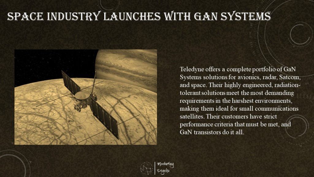
Teledyne offers a complete portfolio of GaN Systems solutions for avionics, radar, Satcom, and space. Their highly engineered, radiation-tolerant solutions meet the most demanding requirements in the harshest environments, making them ideal for small communications satellites. Their customers have strict performance criteria that must be met, and GaN transistors do it all.
Silicon has reached its limitations in solving critical power systems challenges. GaN transistors are the solution for driving more robust growth and product innovation in space applications, enabling lighter, smaller, lower cost, and more efficient power systems.
The power supplies for spaceborne applications must meet strict size limitations while also handling harsh environments. While some traditional silicon-based solutions have been radiation enhanced to tolerate the environment beyond the Earth’s protective shield, they are typically more expensive at both the component and system level, have reduced power density, and result in greater system weight. GaN transistors offer faster power supply switching frequencies, resulting in higher power density, higher efficiency, and more compact and lighter weight circuitry. In addition, GaN is inherently radiation tolerant, another key attribute of GaN transistors used in high-altitude and space applications.
GaN also offers significant cost reductions, enabling organizations to design products that provide high performance while using less material. The result is lighter-weight systems and lower-cost launches. For example, while launches cost the average US $18,500 per kilogram in 2000, this has dropped to approximately US $2,700 per kilogram. NASA is targeting $200 per kilogram and implementing GaN can help achieve that target. GaN-powered devices deliver the efficiency, size, and power-density benefits required for demanding HiRel power space applications and helping change the way we explore space. Learn more about where GaN Systems power semiconductors are being used in our white paper: 2021 Top Technology Predictions in Power Electronics.
Transphorm Closes JV Transaction for Acquisition of AFSW Wafer-Fab
Transphorm, a supplier of gallium nitride (GaN) power conversion products, has close of the transaction for the acquisition of 100% interest in the company’s AFSW wafer-fab facility by GaNovation, Transphorm’s recent joint venture with Palo Alto-based JCP Capital, a new strategic-financial partner.
This is a big step forward for Transphorm and its existing AFSW wafer-fabrication facility, previously a JV with Fujitsu Semiconductor Limited (FSL), located in Aizu Wakamatsu, Japan. The facility is a premier wafer manufacturing fab for high quality, reliable high voltage GaN power semiconductors.
The transaction completes the planned exit of Fujitsu Semiconductor from the AFSW fab. Transphorm’s effective stake in AFSW will be 25% (via its 25% ownership of GaNovation), down from its previous 49% stake. This will reduce Transphorm’s direct capital outlay for AFSW by approximately 50%, resulting in more efficient P&L, with investment in GaN technologies and applications. In addition, partnering with JCP Capital adds a significant strategic-financial partner for AFSW that has global strength in the GaN ecosystem.
“We are delighted to partner with Transphorm in AFSW, and its new parent entity GaNovation, a joint venture with Transphorm,” says David Cong, Founder and Managing Partner, JCP Capital, in a press release. “GaNovation will not only bring significant capital to AFSW, the world’s premier GaN power wafer fab, over the next several years to expand GaN wafer manufacturing, but also contribute to growing the GaN product business together with our portfolio ecosystem at a faster vector, especially in the area of GaN-based fast chargers and adapters.”
Primit Parikh, co-founder and President of Transphorm, adds, “The partnership with GaNovation and JCP Capital is the ideal next step in Transphorm’s rapid growth and manufacturing of its highest quality-highest reliability GaN wafers and products, continuing our asset-light vertically integrated model with strong IP dominance and protection. We also thank Fujitsu Semiconductor for its long-standing partnership as well as its commitment to assist in the successful transition of AFSW going forward.”
Macronix and Foxconn Sign Asset Transaction Agreement for 6-inch Wafer Fab
Macronix International Co., Ltd. (“Macronix”), a leading integrated device designer and manufacturer in Non-Volatile Memory (NVM), and Hon Hai Technology Group (“Foxconn”), the world’s largest electronics manufacturer and service provider, announced the signing of an Asset Transaction Agreement for the sales of Macronix’s 6-inch wafer fab and equipment in Hsinchu Science Park to Foxconn for NT$2.52 billion. The transaction is expected to be closed by the end of 2021.
The Asset Transaction Agreement was signed by Dr. Chih-Yuan Lu, President of Macronix, and Dr. Bob Wei-Ming Chen, President of Foxconn Semiconductor Business Group (“S Business Group”). The momentous event was also witnessed by Mr. Miin Wu, Chairman and CEO of Macronix, and Mr. Young Liu, Chairman and CEO of Foxconn. Not only does the transaction reflect Foxconn’s commitment to the long-term “3+3” (industry and technology) company vision but it also signifies a deeper commercial collaboration between Macronix and Foxconn.
“The acquisition of the 6-inch wafer fab in Hsinchu Science Park officially signals Foxconn’s entry into the manufacture and development of wide band gap semiconductors, especially SiC, paving the way for a long-term commitment to semiconductor development. The manufacturing of SiC is in line with Foxconn’s 3+3 strategy (EV, digital health, Robotics + AI, semiconductor, advanced communication). SiC MOSFET is an important device for EV, while EV occupies the No.1 position in Foxconn’s 3+3 strategy. The 6-inch wafer fab will function as S Business Group’s headquarters in Hsinchu, the world famous semiconductor cluster, enabling closer partnership with the semiconductor companies based in the Hsinchu Science Park”, said Mr. Young Liu, Chairman and CEO of Foxconn.
“To enhance advanced technology and global competitiveness, Macronix will focus on 12-inch wafer business, especially R&D and manufacturing of the advanced 3D NAND Flash and NOR Flash products after capacity expansion. Macronix is pleased to see the subject 6-inch wafer fab continue to make its contribution to Taiwan as Foxconn commits to have the fab be used as an important base for Foxconn to reinforce its semiconductor development plan and to meet the demand of electric vehicles. Considering that Macronix is advancing to take the lead in the global automotive electronics market, a closer collaboration between Macronix and Foxconn in the near future may be anticipated”, said Mr. Miin Wu, Chairman and CEO of Macronix.
The interim Board meeting was held by Macronix and Foxconn respectively this morning to approve the above transaction, and the contract signing ceremony was held shortly at the subject 6-inch wafer fab. The subject 6-inch wafer fab, located in Hsinchu Science Park with completed industrial supply chain. In addition to manufacture SiC Power MOSFET, Foxconn confirmed that it will also manufacture silicon wafer products, such as MEMS, in order to achieve Foxconn’s strategic goals on development of semiconductors industry, electric vehicles, and digital health.
Subscribe to Power Semiconductors Weekly and watch it on YouTube every Tuesday.
If you prefer a monthly update about the world of power semiconductors delivered to your e-mail address, please, subscribe to Marketing Psycho Power Semiconductors newsletter.