Power Semiconductors Weekly Vol. 17
Industry’s First Automotive Qualified SiC Six-Pack Power Module for EV Traction Inverters – Easy Power Upscaling with HybridPACK™ Drive CoolSiC™
Infineon Technologies AG introduced a new automotive power module with CoolSiC™ MOSFET technology. At this year’s virtual PCIM trade show, Infineon presented the new HybridPACK™ Drive CoolSiC™, a full-bridge module with 1200 V blocking voltage optimized for traction inverters in electric vehicles (EV). The power module is based on the automotive CoolSiC trench MOSFET technology for high-power density and high-performance applications. This offers higher efficiency in inverters with longer ranges and lower battery costs, particularly for vehicles with 800 V battery systems and larger battery capacity.
The new HybridPACK Drive CoolSiC is in production now and will be available starting June 2021.
The HybridPACK Drive was first introduced in 2017, using Infineon’s silicon EDT2 technology, specifically optimized to deliver the best efficiency on a real-world driving cycle. It offers a scalable power range of 100 kW to 180 kW within the 750 V and 1200 V class. This product is Infineon’s market-leading power module with a track record of more than one million pieces shipped for more than 20 electric vehicle platforms. The new CoolSiC version is based on Infineon’s silicon carbide trench MOSFET structure. Compared to planar structures, the trench structure enables a higher cell density, resulting in the best-in-class figure of merit. Therefore, trench MOSFETs can be operated at lower gate-oxide field strengths, resulting in increased reliability.
The power module offers an easy upscale path from silicon to silicon carbide with the same footprint. This allows the inverter design to achieve higher power of up to 250 kW in the 1200 V class, greater driving range, smaller battery size and optimized system size and cost. In order to offer an optimal cost-performance ratio for different power levels, this product is available in two versions with different chip counts, resulting in either a 400 A or 200 A DC rating version in the 1200 V class.
CISSOID Expands Its SiC Intelligent Power Modules Platform
CISSOID, the leader in high temperature Semiconductors and Power Modules, is adding to its growing platform of 3-Phase Silicon Carbide (SiC) MOSFET Intelligent Power Module (IPM) products by introducing new liquid-cooled modules for E-mobility tailored for lower switching losses or for higher power. The company is also introducing a module based on a lightweight AlSiC flat baseplate that meets the demand for natural convection or forced cooling in aerospace and in dedicated industrial applications. These products integrate a 3-Phase SiC MOSFET module with a powerful gate driver.
These new IPMs leverage a technology platform that can be rapidly adapted to new voltage, power and cooling requirements. They greatly accelerate the design of SiC-based power converters enabling high efficiency and high power density. The embedded gate driver solves multiple challenges related to fast-switching SiC transistors: negative drive and Active Miller Clamping (AMC) prevent parasitic turn-on; Desaturation detection and Soft-Shut-Down (SSD) react rapidly but safely to short-circuit events; Undervoltage Lockout (UVLO) functions on gate driver and DC bus voltages monitor the proper operation of the system.
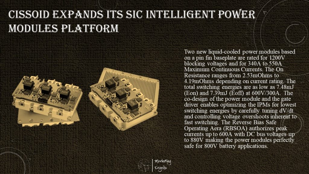
Two new liquid-cooled power modules based on a pin fin baseplate are rated for 1200V blocking voltages and for 340A to 550A Maximum Continuous Currents. The On Resistance ranges from 2.53mOhms to 4.19mOhms depending on current rating. The total switching energies are as low as 7.48mJ (Eon) and 7.39mJ (Eoff) at 600V/300A. The co-design of the power module and the gate driver enables optimizing the IPMs for lowest switching energies by carefully tuning dV/dt and controlling voltage overshoots inherent to fast switching. The Reverse Bias Safe Operating Aera (RBSOA) authorizes peak currents up to 600A with DC bus voltages up to 880V making the power modules perfectly safe for 800V battery applications.
Imec and AIXTRON Demonstrate 200 mm GaN Epitaxy on AIX G5+ C for 1200V Applications with Breakdown in Excess of 1800V
Imec, a world-leading research and innovation hub in nanoelectronics and digital technologies, and AIXTRON, the leading provider of deposition equipment for compound semiconductor materials, have demonstrated epitaxial growth of gallium-nitride (GaN) buffer layers qualified for 1200V applications on 200mm QST® substrates, with a hard breakdown exceeding 1800V. The manufacturability of 1200V-qualified buffer layers opens doors to highest voltage GaN-based power applications such as electric cars, previously only feasible with silicon-carbide (SiC)-based technology. The result comes after the successful qualification of AIXTRON’s G5+ C fully automated metal-organic chemical vapor deposition (MOCVD) reactor at imec, Belgium, for integrating the optimized material epi-stack.
Wide-bandgap materials gallium-nitride (GaN) and silicon-carbide (SiC) have proved their value as next-generation semiconductors for power-demanding applications where silicon (Si) falls short. SiC-based technology is the most mature, but it is also more expensive. Over the years tremendous progress has been made with GaN-based technology grown on for example 200mm Si wafers. At imec, qualified enhancement mode high-electron-mobility transistors (HEMTs) and Schottky diode power devices have been demonstrated for 100V, 200V and 650V operating voltage ranges, paving the way for high-volume manufacturing applications. However, achieving operating voltages higher than 650V has been challenged by the difficulty of growing thick-enough GaN buffer layers on 200mm wafers. Therefore, SiC so far remains the semiconductor of choice for 650-1200V applications – including for example electric cars and renewable energy.
For the first time, imec and AIXTRON have demonstrated epitaxial growth of GaN buffer layers qualified for 1200V applications on 200mm QST® (in SEMI standard thickness) substrates at 25°C and 150°C, with a hard breakdown exceeding 1800V. Denis Marcon, Senior Business Development Manager at imec: “GaN can now become the technology of choice for a whole range of operating voltages from 20V to 1200V. Being processable on larger wafers in high-throughput CMOS fabs, power technology based on GaN offers a significant cost advantage compared to the intrinsically expensive SiC-based technology.”
On Semi Brings Silicon Carbide to Formula E Power Inverter
Power inverters made using silicon carbide improve a car’s performance while also allowing increased torque and acceleration. ON Semiconductor is participating in the Formula E World Championship with a partnership with the Mercedes-EQ Formula E team on the development of next-generation electric powertrains equipped with SiC inverters.
The technical collaboration between ON Semiconductor and Mercedes AMG’s High Power Performance (HPP) division has provided technological advances for race cars. In an interview with EE Times, ON Semiconductor vice president, global systems engineering, highlighted how design and testing go hand in hand in Formula E, enabling the continuous improvement of the inverter power stages.
“When we started in Formula E, we came in as a sponsor, working only with the Mercedes team, and we were looking for some ways to show what we did and are doing for the electronic vehicles (EV) market,” said Priscak. “But very quickly, working with their development team, we realized that there is a lot we can learn from each other from an engineering perspective. And so it became more of a partnership than a sponsorship. Our design engineers are working with the powertrain engineers at Formula E to develop the next generation of traction inverters and power transfer systems for Formula E. Most of what we learn can be applied to commercial solutions but the torque ratios are very different from what you find in a normal car.”
NXP Sells $2 Billion of Debt to Fund Power-Saving Semiconductors
NXP Semiconductors NV sold $2 billion of bonds to help finance the development of semiconductors that reduce energy consumption in products like power adapters and electric vehicles.
The chipmaker issued bonds in two parts. The longer portion of the deal, a 20-year security, yields 1.15 percentage points above Treasuries, down from the initially targeted 1.5% premium. That equates to about 3.30%.
The money will partly fund research and development for innovation in green chips, battery control and energy management for electric and hybrid cars, smart-building technologies, as well as energy-efficiency measures at NXP’s own facilities. The funds were raised by subsidiaries NXP B.V., NXP Funding LLC and NXP USA Inc. The company raised $1 billion in green debt in April 2020.
Corporations and governments globally have raised about $156 billion from green bonds this year, nearly tripling the roughly $58 billion issued over the same span in 2020, according to data compiled by Bloomberg. The technology sector hasn’t been a huge contributor, amounting to only 1.2% of this year’s total.
Infineon Increases Supply Security for Silicon Carbide by Expanding the Supplier Base
Infineon Technologies AG has concluded a supply contract with the Japanese wafer manufacturer Showa Denko K.K. for an extensive range of silicon carbide material (SiC) including epitaxy. The German semiconductor manufacturer has thus secured more base material for the growing demand for SiC-based products. SiC enables highly efficient and robust power semiconductors that are used in particular in the fields of photovoltaic, industrial power supply, and charging infrastructure for electric vehicles.
The contract between Infineon and Showa Denko K.K. has a two-year term with an extension option.

“Our broad and fast growing portfolio demonstrates Infineon’s leading role in supporting and shaping the market for SiC-based semiconductors which is expected to grow 30 to 40 percent annually over the next five years”, says Peter Wawer, President of the Industrial Power Control Division at Infineon. “The expansion of our supplier base with Showa Denko for wafers in this growth market marks an important step in our multisourcing strategy. It will support us to reliably meet the growing demand mid to longterm. Furthermore, we plan to collaborate with Showa Denko on the strategic development of the material to improve the quality while cutting costs at the same time.”
“We are proud to be able to provide Infineon with Best-in-Class SiC material and our cutting-edge epitaxy technology” says Jiro Ishikawa, Senior Managing Corporate Officer from Showa Denko K.K.. “Our aim is to continuously improve our SiC material and develop the next technology. We value Infineon as an excellent partner in this regard.”
Industry Alliance Crucial to SiC Advancement in Taiwan, Says Actron Chair
Taiwan has lagged behind world leaders by 20-30 years in the development of third-generation semiconductor materials including silicon carbide (SiC) and must use more collective forces to accelerate the advancement in the segment, according to MK Lu, chairman of automotive diode maker Actron Technology.
Lu, speaking at the inauguration ceremony for Taiwan Compound Semiconductor Alliance, said that he hopes more manufacturers will join the alliance to build a strong ecosystem covering diverse aspects ranging from equipment, materials, and epi wafers to wafer foundry and terminal applications.
China has decided to invest CNY4 trillion (US$618.24 billion), and Japan CNY10 trillion (US$91.19 billion), in the development of new-generation compound semiconductors, said Lu, who is also honorary chairman of Sino-American Silicon Products (SAS). He expressed hopes that Taiwan’s Ministry of Science and Technology and Ministry of Economic Affairs can inject more resources to help the industry root deeper and catch up with world leaders.
Under Lu’s efforts, SAS has acquired stakes in GaAs foundry Advanced Wireless Semiconductor (AWSC) and is also joining forces with AWSC, GlobalWafers, Actron and epi wafer foundry Episil Holding to build high-capacity SiC MOSFET and IGBT components for automotive applications.
Lu said Actron will be ramping up production capacity for SiC MOSFETs in 2022-2023 for use in hybrid vehicles with 48V and 80V power systems, and will continue to roll out with partners silicon-based IGBT modules with 600V, 750V and 1,200 V in power capacity for future pure electric vehicles (BEV).
Lu continued that both Win Semiconductors and AWSC can tap deeper into the higher-end field of high-frequency RF chips foundry for 5G and even 6G wireless communication applications.
Lu also noted SAS silicon wafer subsidiary GlobalWafers has been also engaged in the compound semiconductor sector for eight years, starting with production of 4-inch N-type conductive SiC wafers in cooperation with Win Semi and now able to produce 6-inch conductive and semi-insulated offerings.
Lu continued that GlobalWafers has also teamed up with US-based GT Advanced Technologies (GTAT) to forge a new supply source of 6-inch SiC wafers, which are manufactured from bulk SiC crystal produced by GTAT.
Find more information about power semiconductors in Marketing in Power Electronics section of the website.