Power Semiconductors Weekly Vol. 119
Toshiba Releases 600V Super Junction Structure N-Channel Power MOSFET
Toshiba Electronic Devices & Storage Corporation (“Toshiba”) has expanded its line-up of N-channel power MOSFETs fabricated with the latest-generation process, with a 600V super junction structure suitable for data centers, switching power supplies, and power conditioners for photovoltaic generators. The new product, “TK055U60Z1,” is the first 600V product in the DTMOSVI series.
By optimizing the gate design and process, 600V DTMOSVI series products reduce drain-source On-resistance per unit area by approximately 13%, and drain-source On-resistance × gate-drain charge, the figure of merit for MOSFET performance, by approximately 52%, compared to Toshiba’s current generation DTMOSIV-H series products with the same drain-source voltage rating. This ensures the series achieve both low conduction loss and low switching loss, and helps to improve efficiency of the switching power supplies.
The new product is housed in a TOLL package that allows Kelvin connection of its signal source terminal for the gate drive. The influence of inductance in the source wire in the package can be reduced to accentuate the high-speed switching performance of the MOSFET, which suppresses oscillation during switching.
Toshiba will continue to expand its 600V DTMOSVI series line-up, and its already released 650V DTMOSVI series products, and support energy conservation by reducing power loss in switching power supplies.
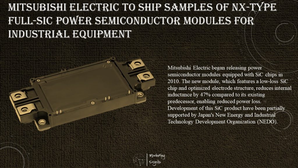
Mitsubishi Electric to Ship Samples of NX-type Full-SiC Power Semiconductor Modules for Industrial Equipment
Mitsubishi Electric Corporation announced that it will begin shipping samples of its new NX-type full-SiC (silicon carbide) power semiconductor module for industrial equipment on June 14. The module, which reduces internal inductance and incorporates a second-generation SiC chip, is expected to contribute to the realization of more efficient, smaller and lighter-weight industrial equipment.
Power semiconductors are increasingly being utilized to convert electric power extra efficiently and thereby help to lower the carbon footprint of global society. Expectations are particularly high for SiC power semiconductors because of their capability to significantly reduce power loss. The demand is expanding for high-power, high-efficiency power semiconductors capable of improving the power-conversion efficiency of components such as inverters used in industrial equipment.
Mitsubishi Electric began releasing power semiconductor modules equipped with SiC chips in 2010. The new module, which features a low-loss SiC chip and optimized electrode structure, reduces internal inductance by 47% compared to its existing predecessor, enabling reduced power loss. Development of this SiC product have been partially supported by Japan’s New Energy and Industrial Technology Development Organization (NEDO).
Infineon Releases Next Generation 1200 V CoolSiC™ Trench MOSFET in TO263-7 Package to Boosts e-Mobility
Infineon presents its new generation of 1200 V CoolSiC™ MOSFETs in TO263-7 for automotive applications. The automotive-graded silicon carbide (SiC) MOSFET generation offers high power density and efficiency, enables bi-directional charging and significantly reduces system cost in on-board charging (OBC) and DC-DC applications.
The 1200 V CoolSiC family member offers best-in-class switching performance through 25 percent lower switching losses compared to the first generation. This improvement in switching behavior enables high-frequency operation, leading to smaller system sizes and increased power density. With a Gate-source threshold voltage (V GS(th)) greater than 4 V and a very low Crss/ Ciss ratio, reliable turn-off at V GS = 0 V is achieved without the risk of parasitic turn-ons. This allows for unipolar driving, resulting in reduced system cost and complexity. In addition, the new generation features a low on resistance (R DS(on)), reducing conductive losses over the whole temperature range of -55°C to 175°C.
The advanced diffusion soldering chip mount technology (.XT technology) significantly improves the package’s thermal capabilities, lowering the SiC MOSFET junction temperature by 25 percent compared to the first generation.
Moreover, the MOSFET has a creepage distance of 5.89 mm, meeting 800 V system requirements and reducing coating effort. Infineon is offering a range of R DS(on) options to cater to diverse application demands, including the only 9 mΩ type in the TO263-7 package currently on the market.
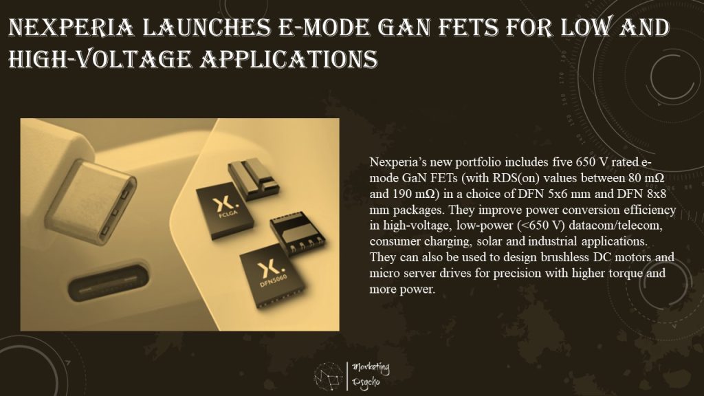
Nexperia Launches E-mode GaN FETs for Low and High-voltage Applications
Nexperia released its first Power GaN FETs in e-mode (enhancement mode) configuration for low (100/150 V) and high (650 V) voltage applications. By augmenting its cascode offering with seven new e-mode devices, Nexperia now provides designers with the optimum choice of GaN FETs from a single supplier alongside its substantial portfolio of silicon-based power electronics components.
Nexperia’s new portfolio includes five 650 V rated e-mode GaN FETs (with RDS(on) values between 80 mΩ and 190 mΩ) in a choice of DFN 5×6 mm and DFN 8×8 mm packages. They improve power conversion efficiency in high-voltage, low-power (<650 V) datacom/telecom, consumer charging, solar and industrial applications. They can also be used to design brushless DC motors and micro server drives for precision with higher torque and more power.
Nexperia now also offers a 100 V (3.2 mΩ) GaN FET in a WLCSP8 package and a 150 V (7 mΩ) device in a FCLGA package. These devices are suitable for various low-voltage (<150 V), high-power applications to deliver, for example, more efficient DC-DC converters in data centers, faster charging (e-mobility and USB-C), smaller LiDAR transceivers, lower noise class D audio amplifiers and more power dense consumer devices like mobile phones, laptops, and games consoles.
GaN FETs offer the highest power efficiency with the most compact solution size in many power conversion applications, features which substantially reduce the bill of materials (BOM). As a result, GaN devices are increasingly entering mainstream power electronics markets, including server computing, industrial automation, consumer, and telecom infrastructure. GaN-based devices offer the fastest transition / switching capability (highest dv/dt and di/dt) and deliver superior efficiency in low- and high-power conversion applications. The outstanding switching performance of Nexperia’s e-mode GaN FETs is attributable to very low Qg and QOSS values, while their low RDS(on) enables more power-efficient designs.
With this release Nexperia now supply a broad offering of GaN FET products to suit the wide range of power applications best suited to the technology, including cascode devices for high-voltage, high-power applications, 650 V e-mode devices for high-voltage, low-power applications and 100/150 V e-mode devices for low-voltage, high-power applications.
Furthermore, Nexperia e-mode GaN FETs are fabricated on an 8” wafer-line for increased capacity and qualified for industrial applications according to JEDEC standard. The expansion of its GaN device offering is a testament to Nexperia’s commitment to quality silicon and wide-bandgap technologies.
SK Powertech Adopts Silvaco’s Victory TCAD Solution for the Development of NextGen SiC Power Devices
Silvaco Group, Inc. (“Silvaco”), a provider of TCAD, EDA software, and design IP, announced that SK Powertech has adopted its Victory TCAD (Technology Computer-Aided Design) solution for power devices to accelerate research and development of its next generation SiC (Silicon Carbide) power devices. The Victory TCAD solution enables SK Powertech to achieve significant improvements in its power management technology.
SK Powertech is a leading provider of compact SiC power devices for high voltage/high temperature applications serving growing end markets such as electric vehicles, railways, and alternative energy. SK Powertech’s products are optimal for smaller, light-weight packages with high voltage/high temperature requirements.
“To achieve significant advances in SiC power semiconductor performance, we sought a partner who could assist us in implementing our next-generation SiC power technology. Through our collaboration with Silvaco’s technical team and the utilization of their Victory TCAD Solution for power devices, we successfully transformed conceptual ideas into actual working devices,” said Dr. Changheon Yang, director of R&D center at SK Powertech. “The combination of the advanced feature set in Victory TCAD Solution and Silvaco’s depth of technical capabilities enables us to deliver the best products and to meet our end market requirements.”
“The expanding markets for power management in solar, automotive, industrial applications and embedded computers are driving the growing adoption of SiC power devices,” said Dr. Babak Taheri, CEO of Silvaco Group. “The success of SK Powertech demonstrates the benefits of using Silvaco Victory TCAD solution for power devices. This solution enables the development of cutting-edge semiconductor products that drive innovation and advancement in the field.”
“Our Victory TCAD solution is recognized in the semiconductor industry for its simulation and analyses capabilities and is widely adopted in the SiC power devices market,” said Eric Guichard, Senior Vice President, and General Manager of the TCAD business unit of Silvaco. “With Silvaco’s TCAD solution, SK Powertech is well-positioned to make significant advancements in SiC power device technology and to contribute to the adoption of its SiC devices in various industries.”
Chinese Cities Back Compound Semiconductor Industry as Demand Grows
Several Chinese cities have been supporting the development of the compound semiconductor industry amid surging demand for new energy vehicles, mobile phone base stations, data centers, and rail transit. Wuxi has chosen compound semiconductors as one of the five industries it plans to focus on in the future. The city in eastern Jiangsu province also intends to make great efforts to develop the production of compound semiconductor materials such as gallium nitride and silicon carbide.
Making compound semiconductors, or chips made from two or more elements, has lower equipment requirements, needs less investment than integrated circuits, and does not rely on processing devices such as high-precision lithography machines, so it is crucial for China to make breakthroughs in this field.
International rivalry has escalated from product and enterprise competition to industrial chain competition, and the next two to three years are critical for the development of the compound semiconductor industry, according to Gan Yong, an academician at the Chinese Academy of Engineering.
Changsha in central Hunan province will introduce policies to issue a total of CNY50 million (USD7.2 million) worth of subsidies to support the semiconductor and IC industries, including third-generation semiconductors.
Guangdong, the province with China’s biggest regional economy, plans to set up a CNY30 billion (USD4.4 billion) fund to invest in automotive chips, semiconductor material devices, and compound semiconductors. The southern province has already built compound semiconductor production lines in the cities of Guangzhou, Shenzhen, Zhuhai, and Dongguan.
Wuhan’s Donghu New Technology Development Zone will build a compound semiconductor industrial chain based in its Jiufengshan Science Park and Jiufengshan Laboratory, the area also known as Optics Valley recently announced.
As one of China’s four IC industry bases, Optics Valley has developed toward two industrial directions, storage and optical chips, with the scale of the latter accounting for half of the country’s total. It boasts more than 30,000 engineering technology and research talents in the semiconductor field.
Wuhan said it will offer investment subsidies of as much as CNY500 million (USD72.4 million) and innovation allowances of up to CNY30 million for the IC industry. More than 100 companies in the IC industrial chain are expected to be based in the Jiufengshan Science Park by 2025.
Subscribe to Power Semiconductors Weekly and watch it on YouTube every Tuesday.
If you prefer a monthly update about the world of power semiconductors delivered to your e-mail address, please, subscribe to Marketing Psycho Power Semiconductors newsletter