Power Semiconductors Weekly Vol. 118
GE Scientists Demonstrate Ultra-High Temperature SiC MOSFET Electronics
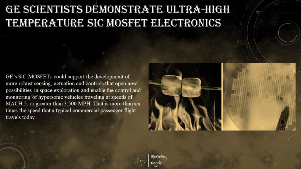
A team of scientists from GE Research have set a new record, demonstrating SiC MOSFETs (Metal–Oxide–Semiconductor Field-Effect Transistors) that can tolerate temperatures exceeding 800 degrees C. This at least 200 degrees C higher than previously known demonstrations of this technology and shows the potential of SiC MOSFETs to support future applications in extreme operating environments. It also defies what most electronics experts believed was achievable with these devices.
As GE’s Aerospace business looks to continuously improve the state-of-the-art in aviation systems for its existing commercial and military customers and seeks to enable new applications in support of space exploration and hypersonic vehicles, building a portfolio of electronics that can function in extreme operating environments will be essential. For more than three decades, GE has built a world leading portfolio in SiC technology and sells an array of SiC-based electrical power products through the Aerospace business for aerospace, industrial and military applications.
Emad Andarawis, a Principal Engineer in Microelectronics at GE Research, says achieving the high temperature threshold with SiC MOSFETs could open a whole new aperture of sensing, actuation and control applications for space exploration and hypersonic vehicles, stating, “We know that to break new barriers with space exploration and hypersonic travel, we will need robust, reliable electronics systems that can handle the extreme heat and operating environments. We believe that we have set a record, demonstrating 800 degree C SiC MOSFETS that represents a key milestone toward these mission critical goals.”
GE’s SiC MOSFETs could support the development of more robust sensing, actuation and controls that open new possibilities in space exploration and enable the control and monitoring of hypersonic vehicles traveling at speeds of MACH 5, or greater than 3,500 MPH. That is more than six times the speed that a typical commercial passenger flight travels today.
Andarawis noted that the electronics industry has seen a number of exciting developments in high temperature electronics with SiC. The National Aeronautics and Space Administration (NASA) has demonstrated SiC JFETs that have tolerated well beyond the 800 degree C threshold. For a long time, the conventional wisdom has been that SiC MOSFETs cannot offer the same degrees of reliability and durability as JFETs at high temperatures. New advancements with the gate oxides in SiC MOSFETS, which have previously been temperature and lifetime limiters, have narrowed the gap considerably.
The recent demonstration of Andarawis and the GE Research shows that MOSFETs could expand the portfolio of available options to consider. This builds on a growing body of work in SiC-enabled electronics that GE Aerospace researchers are at the forefront of leading. The team is currently collaborating on a project with NASA to apply novel SiC photodiode technology to develop and demonstrate a Ultraviolet imager that enhances space missions to the surface of Venus. GE research teams also are fabricating NASA’s JFETs in our cleanroom facility as part of work they are doing for an external semiconductor partner.
The cleanroom facility is a major focal point of GE’s research in SiC. It is a 28,000 sq. ft., Class 100 (ISO 9001 certified) facility, based on GE’s research campus in Niskayuna, NY. The facility can support technology from R&D through low-volume production and transfer technology to high-volume manufacturing supporting GE internal products or select external commercial partners (www.ge.com/research/).
Andawaris said, “GE’s Cleanroom facility is a tremendous research, prototyping and production asset that is allowing us to rapidly develop and scale promising electronics platforms like SiC MOSFETs. We are excited about the road ahead as we support GE Aerospace’s efforts to redefine air travel in the skies and beyond.”
Simulation Model of Industry’s First 1200 V GaN-on-Sapphire Device Released by Transphorm
Transphorm, Inc. announced availability of its 1200 V FET simulation model and preliminary datasheet. The TP120H070WS FET is the only 1200 V GaN-on-Sapphire power semiconductor introduced to date, making its model the first of its kind. Its release indicates Transphorm’s ability to support future automotive power systems as well as three-phase power systems typically used in the broad industrial, datacom, and renewables markets. These applications will benefit from the 1200 V GaN device’s higher power density and reliability along with equal or better performance at more reasonable cost points versus alternative technologies.
Transphorm recently validated the GaN device’s higher performance ability in a 5 kW 900 V buck converter switching at 100 kHz. The 1200 V GaN device achieved 98.7% efficiency, exceeding that of a similarly rated production SiC MOSFET.
The innovative 1200 V technology also underscores Transphorm’s leadership in GaN power conversion. Vertical integration, epitaxy ownership, and patented process paired with decades of engineering expertise enable the company to bring to market the highest performing GaN device portfolio with four additional major differentiators: Manufacturability, Drivability, Designability, and Reliability.
Transphorm’s 1200 V technology is anchored in proven process and mature technology, satisfying customer confidence requirements. The GaN-on-Sapphire process is in volume production today in the LED market. Additionally, the 1200 V technology leverages the fundamentally superior, normally-off GaN platform used in Transphorm’s current device portfolio.
Key TP120H070WS device specifications include:
- 70 mΩ RDS(on)
- Normally off
- Efficient bidirectional current flow
- ± 20 Vmax gate robustness
- Low 4Vth gate drive noise immunity
- Zero QRR
- 3-lead TO-247 package
The Verilog-A device model is recommended for use with the SIMetrix Pro v8.5 Circuit Simulator. A LTSpice model is in development and will be released in Q4 2023. Simulation modeling allows for fast and efficient power system design validation while reducing design iterations, development time, and hardware investments.
The device model files and datasheet are available for download here: https://www.transphormusa.com/en/products/#models.
1200 V FET samples are expected to be available by Q1 2024.
Nidec and Renesas Collaborate on Semiconductor Solutions for Next-Generation E-Axle for EVs
Nidec Corporation and Renesas Electronics Corporation have agreed to join forces on the development of semiconductor solutions for a next-generation E-Axle (X-in-1 system) that integrates an EV drive motor and power electronics for electric vehicles (EVs).
Today’s EVs are increasingly adopting the 3-in-1 unit called E-Axle, which integrates a motor, inverter, and gearbox (reduction gear). To realize high-performance and efficiency as well as smaller size, light weight and lower cost, and to accelerate vehicle development, EVs are also integrating power electronics controls such as DC-DC converters and on-board chargers (OBCs). EV manufacturers in advanced markets such as China have developed an X-in-1 platform that integrates multiple functions, accelerating the adoption in many vehicle models.
As X-in-1 integrates multiple functions and increases in complexity, maintaining a high-level of quality in vehicles becomes challenging. Thus, developing preventive safety technologies such as diagnostic functions and failure prediction is crucial for ensuring safety and security in vehicles. To address this challenge, the two companies agreed to combine Nidec’s motor technology and Renesas’ semiconductor technology to jointly develop a highly reliable and high-performance proof of concept (PoC) for the X-in-1 system. The PoC is designed to support the industry’s highest performance and efficiency as well as smaller size, light weight and lower cost for the X-in-1 system.

The companies plan to launch the first PoC by the end of 2023, which will feature a 6-in-1 system with a DC-DC converter, OBC, and power distribution unit (PDU) as well as a motor, inverter, and gearbox. As a second phase in 2024, Nidec and Renesas plan to develop a highly integrated X-in-1 PoC that incorporates a battery management system (BMS) along with other components. The first PoC will include power devices based on SiC (silicon carbide), and the second PoC will replace the DC-DC and OBC power devices with GaN (gallium nitride), offering excellent performance in high-frequency operation, to further reduce size and cost.
Building on the PoC developed through this collaboration, Nidec plans to rapidly productize E-Axle systems to add to its portfolio and ramp up to mass production to lead the E-Axle market.
Renesas plans to develop and deliver turnkey solutions for increasingly complex X-in-1 systems by expanding the jointly developed PoC for E-Axle reference designs.
GlobalFoundries and STMicroelectronics Finalize Agreement for New 300mm Semiconductor Manufacturing Facility in France
GlobalFoundries Inc. and STMicroelectronics announced the conclusion of the agreement to create a new, jointly-operated, high-volume semiconductor manufacturing facility in Crolles (France), which was announced on 11 July 2022.
“I would like to thank Minister Le Maire, the French Minister of the Economy and Finance, and his team for their support and the dedication for the last 12+ months that have made celebrating today’s milestone possible,” said Dr. Thomas Caulfield, president and CEO of GlobalFoundries. “In partnership with ST in Crolles, we are further expanding GF’s presence within Europe’s dynamic technology ecosystem while benefiting from economies of scale to deliver additional capacity in a highly capital efficient manner. Together we will deliver GF’s market leading FDX technology and ST’s comprehensive technology roadmap, in alignment with customer demand which is expected to remain high for Automotive, IoT, and Mobile applications over the next decades.”
“Today marks an important milestone for ST, for GF as well as for Europe. This could not have been achieved without the support of the French government as well as of the European Commission,” said Jean-Marc Chery, President and CEO of STMicroelectronics. “We will further reinforce the European and French FD-SOI ecosystem, building more capacity for our European and global customers in complex, advanced technologies for key end-markets including automotive, industrial, IoT and communication infrastructure, as they transition to digitalization and decarbonization. This new manufacturing facility will support our $20 billion+ revenue ambition.”
The program represents an overall projected cost of 7.5 billion euro for CAPEX, maintenance and ancillary costs. The new facility will benefit from significant financial support from the State of France (administered by Bpifrance). The aid measure, in line with the objectives set out in the European Chips Act and part of the “France 2030” plan, recently received approval from the European Commission.
STMicroelectronics and Sanan Optoelectronics to Advance Silicon Carbide Ecosystem in China
STMicroelectronics and Sanan Optoelectronics announced that they have signed an agreement to create a new 200mm silicon carbide device manufacturing JV in Chongqing, China. The new SiC fab is targeting to start production in Q4 2025 and full buildout is anticipated in 2028, supporting the rising demand in China for car electrification as well as for industrial power and energy applications. In parallel, Sanan Optoelectronics will build and operate separately a new 200mm SiC substrate manufacturing facility to fulfill the JV’s needs, using its own SiC substrate process.
The JV will make SiC devices exclusively for STMicroelectronics, using ST proprietary SiC manufacturing process technology, and serve as a dedicated foundry to ST to support the demand of its Chinese customers.
The total amount for the full buildout of the JV is expected to be about $3.2 billion, including capital expenditures of about $2.4 billion over the next 5 years, which will be financed by contributions from STMicroelectronics and Sanan Optoelectronics, local government support, and loans to the JV.
“China is moving fast towards electrification in Automotive and Industrial and this is a market where ST is already well-established with many engaged customer programs. Creating a dedicated foundry with a key local partner is the most efficient way to serve the rising demand of our Chinese customers. The combination of Sanan Optoelectronics’ future 200mm substrate manufacturing facility with the front-end JV and ST’s existing back-end facility in Shenzhen, China will enable ST to offer our Chinese customers a fully vertically integrated SiC value chain,” said Jean-Marc Chery, President and CEO of STMicroelectronics. “It is an important step to further scale up our global SiC manufacturing operations, coming in addition to our continuing significant investments in Italy and Singapore. This JV is expected to be one of the enablers of the opportunity we see to reach $5B+ SiC revenues by 2030. This initiative is consistent with ST 2025-27 $20B+ revenue ambition and the associated financial model, previously communicated to the financial markets.”
“The establishment of this joint venture will be a major driving force for the wide adoption of SiC devices on the Chinese market,” said Simon Lin, CEO of Sanan Optoelectronics. “Being an international, well-known, high quality SiC foundry service company, Sanan will also supply its SiC substrate to this new joint venture, by building a dedicated new SiC substrate factory. This is an important step for Sanan Optoelectronics’ ambitions as a SiC foundry. With this new Joint Venture and the new SiC substrate capacity expansion, we are confident that we will continue to take the lead in the SiC foundry market.”
The completion of the project is subject to regulatory approvals.
Wolfspeed Webinar: Understanding Wolfspeed’s WolfPACK™ Power Module Family: Your Questions Answered!
Wolfspeed WolfPACK™ modules are a great choice for designers who want to increase efficiency and power density in a compact, industry-standard footprint. The family of modules provides an excellent solution for fast design implementation, scalability, long-term design support, and lower assembly overhead.
Join Wolfspeed for a short technical presentation that covers the WolfPACK™ product family’s internal and external structure, and how recent portfolio expansions enable it to cover a wider range of applications. After this presentation take the opportunity to engage with Wolfspeed’s Dan Martin and Austin Curbow as they host an extended live Q&A session to answer any technical questions relating to the WolfPACK™ module family and how to implement them into your application.
Key Take-Aways:
- Tools to speed and scale up existing designs and what advantages the WolfPACK™ package can provide to achieve your design goals.
- Details about the new full bridge and pre-applied thermal interface material options within the WolfPACK™ family
- Date: June 20, 2023
- Time: 5 PM CEST
Subscribe to Power Semiconductors Weekly and watch it on YouTube every Tuesday.
If you prefer a monthly update about the world of power semiconductors delivered to your e-mail address, please, subscribe to Marketing Psycho Power Semiconductors newsletter