Power Semiconductors Weekly Vol. 115
Mitsubishi Electric to Ship Samples of SBD-embedded SiC-MOSFET Module
Mitsubishi Electric Corporation announced that it will begin shipping samples of a new Schottky barrier diode (SBD)-embedded silicon carbide (SiC) metal-oxide-semiconductor field-effect transistor (MOSFET) module, featuring dual-type 3.3kV withstand voltage and 6.0kVrms dielectric strength. The new module is expected to support superior power, efficiency and reliability in inverter systems for large industrial equipment such as railways and electric power systems.
Mitsubishi Electric has already released four full-SiC modules and two 3.3kV high-voltage dual-type LV100 modules. To further contribute to high power output, efficiency and reliability in inverters for large industrial equipment, the company will soon begin providing samples of its new module, which reduces switching loss as an SiC-MOSFET with a built-in SBD and an optimized package structure.
TI Helps Maximize EV Driving Range with SiC Gate Driver
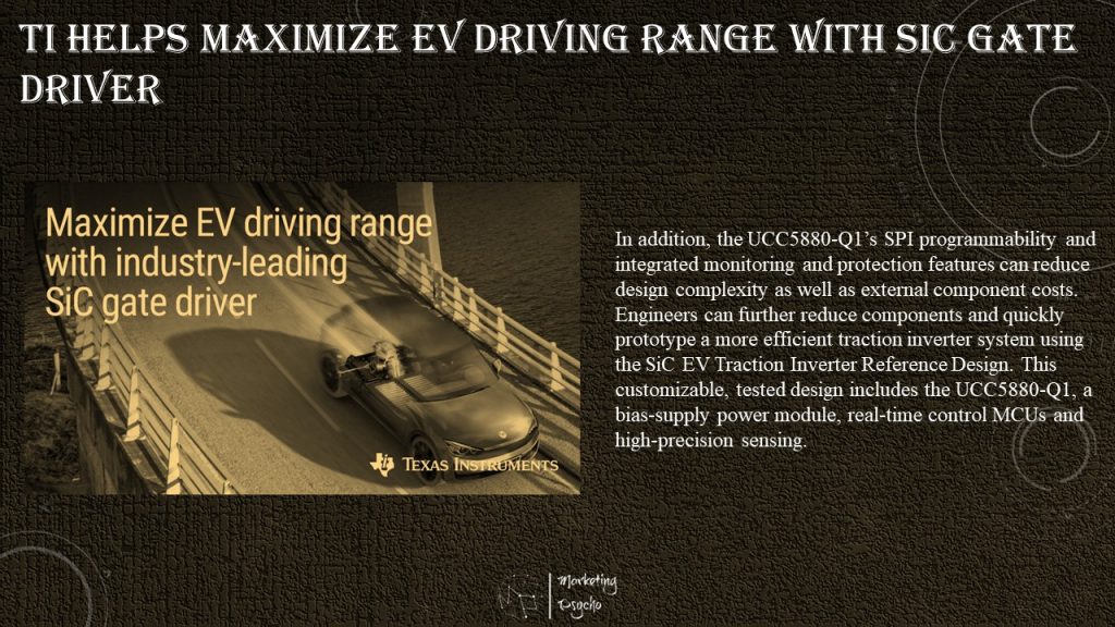
Texas Instruments (TI), a leader in high-voltage technology, debuted a highly integrated, functional safety-compliant, isolated gate driver that enables engineers to design more efficient traction inverters and maximize electric vehicle (EV) driving range. The new UCC5880-Q1 reinforced isolated gate driver offers features that enable EV powertrain engineers to increase power density and reduce system design complexity and cost while achieving their safety and performance goals.
As EVs continue to grow in popularity, semiconductor innovations in traction inverter systems are helping overcome critical barriers to widespread adoption. Automakers can build safer, more efficient and more reliable silicon carbide (SiC)- and insulated-gate bipolar transistor (IGBT)-based traction inverters by designing with UCC5880-Q1, featuring real-time variable gate-drive strength, Serial Peripheral Interface (SPI), advanced SiC monitoring and protection, and diagnostics for functional safety.
“Designers of high-voltage applications like traction inverters face a unique set of challenges to optimize system efficiency and reliability in a small space,” said Wenjia Liu, product line manager for high-power drivers at TI. “Not only does this new isolated gate driver help enable engineers to maximize driving range, but it also integrates safety features to reduce external components and design complexity. And it can be easily paired with other high-voltage power-conversion products such as our UCC14141-Q1 isolated bias supply module to improve power density and help engineers reach the highest levels of traction inverter performance.”
The need for higher reliability and power performance for EVs is continuously growing, as efficiency gains have a direct impact on operating range improvement per charge. But achieving any increase in efficiency is difficult for designers, given that the majority of traction inverters already operate at 90% efficiency or higher.
By varying the gate-drive strength in real time, in steps between 20 A and 5 A, designers can improve system efficiency with the UCC5880-Q1 gate driver as much as 2% by minimizing SiC switching power losses, resulting in up to 7 more miles of EV driving range per battery charge. For an EV user who charges their vehicle three times per week, that could mean more than 1,000 additional miles per year. To learn more, read the technical article, “How to Maximize SiC Traction Inverter Efficiency with Real-Time Variable Gate Drive Strength.”
In addition, the UCC5880-Q1’s SPI programmability and integrated monitoring and protection features can reduce design complexity as well as external component costs. Engineers can further reduce components and quickly prototype a more efficient traction inverter system using the SiC EV Traction Inverter Reference Design. This customizable, tested design includes the UCC5880-Q1, a bias-supply power module, real-time control MCUs and high-precision sensing.
New Innovation Center to Provide AIXTRON with Expanded Capacities for R&D
AIXTRON SE plans to invest up to 100 million euros at its Herzogenrath site. A new innovation center is to be built, which will provide the manufacturer of deposition equipment to the semiconductor industry with enhanced capacities for research and development. AIXTRON received approval for the new project from the company’s Supervisory Board.
The new innovation center will provide 1000m2 of cleanroom space and will be built on the company’s premises in Herzogenrath, Germany. The new building will create further capacities for the next product generations which are already in preparation, as well as for further product developments beyond that.
“With our products, we address the megatrends of digitalization, electromobility and energy efficiency and are experiencing a strong and steadily growing demand. Technical innovations and product developments that precisely address the needs of our customers are the key to our success. And our dynamic environment offers us further growth opportunities,” says Dr. Felix Grawert, CEO of AIXTRON SE. “We are therefore very pleased that the Supervisory Board has approved this project which will enable us to create the foundation for further product developments and for future growth.”
The importance of product development in the dynamic semiconductor industry is demonstrated by the success of AIXTRON’s new “G10” system generations. In the first year after market introduction, AIXTRON expects to generate more than 40 percent of its annual revenues with this new product generation. Right after its official launch, the new tool for the silicon carbide material system (G10-SiC) has already generated a high order intake. And it is expected to continue to drive further growth all throughout 2023 and beyond.
Also, the new AIXTRON solution for the gallium-arsenide/indium-phosphite material system (G10-AsP) which was launched at the beginning of 2023 already enjoys a strong demand. For the first time, it enables the high-volume production of Micro LEDs and photonic components such as lasers on wafers with a diameter of up to 200mm. Later in the year, the new G10 system for gallium nitride (GaN) will also be launched.
The material systems SiC and GaN have the potential to fully cover the complete range of power electronics, from electromobility to renewable energy technologies to fast data transmission. With their outstanding material properties, they will ensure a significant reduction in global CO2 emissions in these areas and help electromobility achieve a breakthrough.
Power Integrations Unveils New SCALE-iFlex LT NTC IGBT/SiC Module Gate Drivers with Temperature Readout
Power Integrations, the leader in gate-driver technology for medium- and high-voltage inverter applications, introduced the SCALE-iFlex™ LT NTC family of IGBT/SiC module gate drivers. The new gate drivers target the popular new dual, 100 mm x 140 mm style of IGBT modules, such as the Mitsubishi LV100 and the Infineon XHP 2, as well as silicon carbide (SiC) variants thereof up to 2300 V blocking voltage. The SCALE-iFlex LT NTC drivers provide Negative Temperature Coefficient (NTC) data – an isolated temperature measurement of the power module – which enables accurate thermal management of converter systems. This is particularly important for systems with multiple modules arrayed in parallel, ensuring proper current sharing and dramatically enhancing overall system reliability.
Thorsten Schmidt, product marketing manager at Power Integrations, commented: “Designers of renewable energy and rail systems using SCALE-iFlex drivers already benefit from increased system performance; the SCALE-iFlex approach handles paralleling so expertly that one module in five can be eliminated without loss of performance or current de-rating. Adding an isolated NTC output reduces hardware complexity – particularly cables and connectors – and contributes to system observability and overall performance.”
Based on Power Integrations’ proven SCALE™-2 technology, SCALE-iFlex LT gate drivers improve current sharing accuracy and therefore increase the current carrying capability of multiple-paralleled modules by 20 percent, allowing users to significantly increase the semiconductor utilization of their converter stacks. This is possible because the localized control of each 2SMLT0220D MAG (Module Adapted Gate driver) unit ensures precise control and switching, enabling excellent current sharing. Advanced Active Clamping (AAC) is employed to deliver accurate overvoltage protection.
To further increase space saving, up to four MAG-driven power modules can be parallel-connected from a single 2SILT1200T Isolated Master Control (IMC) unit, which can also be mounted on a power module due to its compact outline. The gate drivers are fully qualified to IEC 61000-4-x (EMI), IEC-60068-2-x (environmental) and IEC-60068-2-x (mechanical) specifications, and undergo complete type testing – low voltage, high voltage, thermal cycling – shortening designer development time by 12 to 18 months. A comprehensive set of protection features is included, and parts are optionally available with conformal coating.
Penn State and onsemi Sign MOU to Boost Silicon Carbide Research in the U.S.
Penn State and onsemi, a leader in intelligent power and sensing technologies, announced the signing of a memorandum of understanding (MOU) towards an $8 million strategic collaboration which includes the establishment of the onsemi Silicon Carbide Crystal Center (SiC3) at Penn State’s Materials Research Institute (MRI). onsemi will fund SiC3 with $800k per year over the next 10 years.
Silicon carbide (SiC) is vital for enabling efficiency in electric vehicles (EVs), EV charging and energy infrastructure and contributes to the decarbonization of the global economy. Academic research in SiC made great advancements in the late 1990s and early 2000s, but has since diminished in the U.S. This agreement will put SiC crystal research in America back on the map.
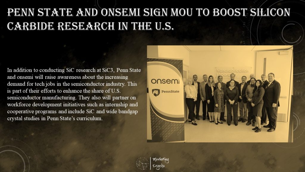
In addition to conducting SiC research at SiC3, Penn State and onsemi will raise awareness about the increasing demand for tech jobs in the semiconductor industry. This is part of their efforts to enhance the share of U.S. semiconductor manufacturing. They also will partner on workforce development initiatives such as internship and cooperative programs and include SiC and wide bandgap crystal studies in Penn State’s curriculum. The relationship with Penn State is part of onsemi’s commitment to promoting STEAM (Science, Technology, Engineering, Arts, and Mathematics) education, ranging from helping K-12 students in underserved communities to university collaborations that support the development of the workforce for today and the future.
Lora Weiss, Penn State senior vice president of research, noted that the Penn State-onsemi collaboration is a match that makes perfect sense given each entity’s demonstrated strengths.
“onsemi is a proven innovator, delivering a comprehensive portfolio of intelligent power and sensing technologies to enable and accelerate sustainable solutions across multiple markets,” Weiss said. “At the same time, as per the National Science Foundation’s research expenditure rankings, Penn State is ranked first in materials science and second in materials engineering. We have world-class nanofab and characterization facilities that support research on thin films, silicon carbide and other materials used in semiconductors and other technologies. These complementary capabilities between onsemi and Penn State will have a strong impact on research and development, economic growth, and workforce development.”
Penn State’s capabilities make them an ideal academic partner for onsemi to advance the state of the art in silicon crystal growth.
“Penn State is uniquely positioned to rapidly establish a silicon carbide crystal growth research program,” said Pavel Freundlich, chief technology officer, Power Solutions Group, onsemi. “The university offers a wide breadth of capability based on its current materials research, wafer processing capabilities in its nanofab facility, and a comprehensive, world-class suite of metrology instrumentation.”
The relationship developed over a period of due diligence during which it became clear that their cooperative efforts would position Penn State and onsemi as leaders in SiC research.
“Over the next decade, this collaboration will enable Penn State to become the nation’s leading resource for semiconductor crystal science and workforce development,” said Justin Schwartz, Penn State executive vice president and provost. “And this would not be possible without the relationship-building efforts of Priya Baboo, senior director of corporate and industry engagement, and the technical expertise of Joshua Robinson, professor of materials science and engineering, and their counterparts at onsemi.”
Scott Allen, vice president, University Relations, onsemi, added that “Penn State’s expansion of its curriculum to offer specialty courses in SiC and wideband gap technology will play a key role in meeting onsemi’s strategic workforce development goals and help to meet American semiconductor workforce goals as outlined in the recently signed CHIPS and Science Act.”
Pioneering Interactive Datasheets from Nexperia Put MOSFET Behavior Analysis at Engineers’ Fingertips
Nexperia announced a significant raising of the bar in semiconductor engineer design support with the release of next-generation interactive datasheets to accompany its Power MOSFETs. By manipulating interactive sliders within the datasheets, users can manually adjust the voltage, current, temperature and other conditions for their circuit application and watch how the operating point of a device dynamically responds to these changes.
These interactive datasheets effectively offer a type of graphical user interface to a circuit simulator, using Nexperia’s advanced electrothermal models to calculate the operating point of a device. In addition, they allow engineers to visualize immediately the interaction between parameters such as gate voltage, drain current, RDS(on) and temperature. Their collective contribution to the device behavior is then displayed dynamically in tables or graphs. As a result, Nexperia’s interactive datasheets can significantly increase productivity by eliminating the time needed for an engineer to perform manual calculations or set up and debug a circuit simulation.
The datasheet is commonly the first port of call when a design engineer is looking to select a device for an application. However, while they contain a wealth of information, including the minimum, maximum and typical specifications across dozens of device parameters, it is often difficult to determine how these are interrelated. Consequently, engineers must perform time-consuming manual calculations or set up a circuit simulator using models provided by the manufacturer (assuming these are available) to thoroughly investigate a device’s behavior. Even then, many manufacturers’ simulation models do not show the effect of temperature changes on device behavior. The new interactive datasheets from Nexperia support engineers by showing real-time interaction across different parameters as they are manually changed with the easy-to-use datasheet sliders.
Chris Boyce, Senior Director of Nexperia’s Power MOSFET business adds, “Whether you are a Design Engineer looking to see how a device will perform at elevated temperature, or a Component Engineer trying to compare devices under different test conditions, our new interactive datasheets are designed to make your life easier.”
The technology powering these datasheets is the same as that used in Nexperia’s hugely successful precision electrothermal MOSFET models, which demonstrate how the behaviour of discrete MOSFETs changes with temperature. The new interactive datasheets are offered in addition to the traditional static datasheets and operate in any standard web browser without the requirement of additional software for device simulation.
With the initial version currently under patent application, Nexperia will be reaching out to its global community of customer engineers to evaluate how interactive datasheets are used in real-time in order to broaden the functionality of future versions.
More than 200 interactive datasheets are already available, covering the devices in Nexperia’s latest generations of Automotive and Industrial Power MOSFETs. Over time, the Company plans to make them available for its entire portfolio of discrete MOSFETs and other devices.
Try a live interactive datasheet in action at nexperia.com/interactive-datasheet
onsemi Considers $2 billion Investment in EV Chip Production
onsemi is considering investing $2 billion in boosting production of silicon carbide chips that are widely used to help extend the range of electric vehicles.
Company executives said during an analyst presentation the company is considering the expansion in either the U.S., the Czech Republic or Korea. The firm already has factories in each of those countries.
onsemi is a longtime supplier to the automotive industry, supplying both chips that go into drive trains of electric cars as well as a broad swath of other chips like cameras and sensors that help with driver-assistance systems.
The company makes more than half of its own chips internally and has invested in a full supply chain for energy efficient silicon carbide chips, making both the raw materials and finished chips in-house.
In an interview, onsemi Chief Executive Hassane El-Khoury said the firm’s silicon carbide chip production is currently centered on one of its factories in Bucheon, South Korea. The company plans to find “end-to-end” production, meaning that whichever site it chooses will transform raw silicon carbide powder into a chip.
El-Khoury said that replicating the entire production process in more than one place has become an important selling point to automakers who are still cautious from 2021, when a freeze in chip-heavy Texas and a shortage from Asian chip suppliers led shutdowns on car production lines.
“It’s always good to have a geographically distributed supply chain,” El-Khoury said.
At a financial analyst day, executives said they aim to capture 40% of the silicon carbide automotive chip market by 2027. The company forecast that growth in that area and others will help it grow revenue at a 10% to 12% compound annual rate, expanding sales from $8.3 billion in 2022 to an estimate with a midpoint of $13.9 billion by 2027.
Over the same time period, onsemi expects to expand free cash flows from $1.6 billion in 2022 to $3.5 billion to $4 billion by 2027.
Subscribe to Power Semiconductors Weekly and watch it on YouTube every Tuesday.
If you prefer a monthly update about the world of power semiconductors delivered to your e-mail address, please, subscribe to Marketing Psycho Power Semiconductors newsletter