Power Semiconductors Weekly Vol. 110
ZF Signs Multi-Year Supply Agreement with STMicroelectronics
The technology group ZF will, from 2025, purchase silicon carbide devices from STMicroelectronics. Under the terms of the multi-year contract, ST will supply a volume of double-digit millions of silicon carbide devices to be integrated in ZF’s new modular inverter architecture going into series production in 2025. ZF will leverage ST’s vertically integrated silicon carbide manufacturing in Europe and Asia to secure customer orders in electromobility.
“With this strategically important step, we are strengthening our supply chain to be able to securely supply our customers. Our order book in electromobility until 2030 now amounts to more than thirty billion euros. For this volume, we need several reliable suppliers for silicon carbide devices,” says Stephan von Schuckmann, member of the ZF Board of Management responsible for electromobility as well as materials management. “In STMicroelectronics, we now have a supplier whose experience with complex systems meets our requirements and who, above all, can produce the devices in exceptionally high quality and at the required quantities.” With this agreement, ZF has gained a world-class supplier for silicon carbide technology, in addition to ZF’s existing partnership agreement on silicon carbide technology announced in February.
“As a vertically integrated company, we are investing heavily to expand capacity and develop our silicon carbide supply chain to support our global and European customers across automotive and industrial sectors, as they pursue electrification and decarbonization targets,” says Marco Monti, President Automotive and Discrete Group of STMicroelectronics. “The key to success in electric vehicle technology is greater scalability and modularity with increased efficiency, peak power, and affordability. Our silicon carbide technologies help deliver these benefits and we are proud to work with ZF, a leading automotive supplier for electrification, to help them differentiate and optimize the performance of their inverters.”
ST will manufacture the silicon carbide chips at its production fabs in Italy and Singapore with packaging of the chips into STPAK, an ST-developed advanced package, and testing at its back-end facilities in Morocco and China.
ST will supply ZF from 2025 with a volume of double-digit millions of third generation silicon carbide MOSFET devices. ZF can connect a variable number of such devices together to match customers’ performance requirements without changing the design of the inverter. Among others, ZF will use the technology in inverters for vehicles of a European car manufacturer whose production start is planned for 2025.
The inverter is the brain of electric drivetrains. It manages the flow of energy from battery to e-motor and vice versa. Inverters have become more efficient and more complex with every development step. The combination of the inverter design and the semiconductors, like silicon carbide, is the key to improving electric vehicle performance. Silicon carbide devices significantly reduce power losses in electric car inverters, as well as in wind turbine and photovoltaic inverters. Devices made with silicon carbide have decisive advantages over conventional silicon-based products, such as higher efficiency, power density and reliability. At the same time, they enable smaller and more cost-effective system designs. Simply put, an electric vehicle charges faster, drives further and has more space when equipped with silicon carbide-based semiconductors.
CIL’s Advanced Semiconductor Packaging Facility Update
It’s been 6 months since CIL announced it’s newly created and UK based advanced semiconductor packaging facility. Contained within the 46,000sq ft facility is a 15,000sq ft ISO7 (Class 10,000) fully qualified cleanroom that is starting to come online and will be ready by late May 2023.
Since last announced, CIL has also taken the decision to segregate part of this cleanroom to add a separate wafer dicing area complete with DISCO DAD3361 dicing saw and all of the necessary ancillary equipment. This equipment is already installed, commissioned and currently running early engineering trials. This wafer dicing equipment and all of CIL’s current micro-electronics and power semiconductor device packaging equipment will then start to transfer out of CIL’s existing facilities in Andover UK from late May 2023 onwards. The equipment and facilities to be transferred are initially the following:
- 1 off DISCO DAD3361 die and device wafer saw system complete with wafer mounting equipment.
- 2 off DATACON 2200EVO Automatic die bonders for power die placement using both SiC & GaN
- 2 off Automatic die bonders
- 2 off manual die bonders
- 5 off ASM 589 Automatic Al wedge bonders
- 2 off ASM EAGLE60 Automatic Au Ball bonders
- 1 off K&S Asterion Heavy Gauge Wedge wire bonder
- 1 off DAGE 4000 die shear/wire bond pull tester
- 1 off DAGE PROSPECTOR die shear/wire bond pull and full diagnostic test system
- 2 off Nordson Asymtek S2-920 Auto dispense systems for auto partial glob top
- 1 off DAGE Quadra7 X-Ray/CT Scan system.
- 1 off Nordson GEN7 Scanning Acoustic Microscope (CSAM)
- 1 off Keyence VHX7000 Digital Microscope with sub-micron laser measurement
- 1 off Boschman Sinterstar Innovate F-XL sinter press for high pressure silver sintering
- 1 off Boschman Pre-heat and cooling tower system for high pressure silver sintering
- 1 off Boschman UNISTAR Auto plastic overmold machine. Capable of BGA’s, LGA’s, QFN’s, Plastic IC’s, Power discrete and Power modules
- 1 off Scheugenpflug VDS U1000 / LP804 VDU Auto epoxy fill system
- 1 off high power 2000W laser welding system for copper busbar welding
- 6 off 3D Printers
- 50 staff of which 30 are engineers
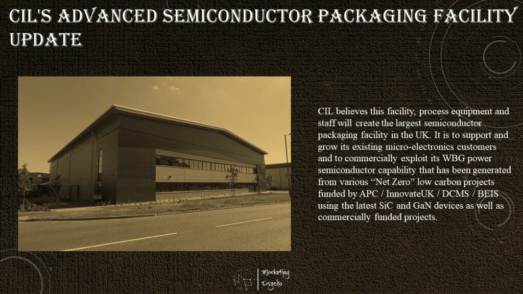
CIL believes this facility, process equipment and staff will create the largest semiconductor packaging facility in the UK. It is to support and grow its existing micro-electronics customers and to commercially exploit its WBG power semiconductor capability that has been generated from various “Net Zero” low carbon projects funded by APC / InnovateUK / DCMS / BEIS using the latest SiC and GaN devices as well as commercially funded projects.
By adding the wafer dicing capability to the facility, CIL will be able to process finished wafers to provide Dicing, Die attach, Wire bonding or power device copper clip attach, glob top, full plastic overmold or potting and back these processes up with inspection equipment that includes, X-Ray, CT-Scan, CSAM, VHX7000, and destructive and non-destructive testing using DAGE 4000 and DAGE PROSPECTOR test stations.
Over the last 3-4 years CIL has grown its engineering department from 8 persons to the 32 persons it has currently and also has a further 10 engineering vacancies. Starting in late May 2023, all of the staff involved in CIL’s semiconductor and power packaging activities will move from CIL’s two existing facilities into this new world class and state of the art semiconductor packaging facility. As with the cleanroom, the offices are nearing completion and will initially house around 30 semiconductor packaging engineers of all levels.
To compliment this semiconductor packaging facility, CIL has also upgraded its existing SMT PCBA equipment consisting of 5 SMT lines and associated 3D AOI, Flying probe test and IPC2 / 3 soldering at its CIL House facility also in Andover UK. This facility totalling 24,000sq ft is being steadily upgraded and added to.
In the last 2 years, CIL has seen its turnover increase from £15M to £27M and headcount increase from 135 persons to 187 persons it has today. Over the next 12 months, as well as bringing on line its advanced semiconductor packaging facility, it will also be adding new processes and equipment to its current PCBA service offering to further support both its customers development and production needs. So with the new packaging facility this will give CIL a total of 80,000sq ft of production space at its three Andover UK sites.
SwissSEM Gets ISO 14001 and ISO 45001 Certifications for Its Production Site
In order to better fulfil customer requirements, improve the company’s internal management and service, enhance the company’s competitiveness, expand market share and establish an excellent corporate image, SwissSEM has decided to start from the second half of 2022, led by the quality department and closely cooperated with all relevant departments, continue to implement environmental management system ISO14001:2015 and occupational health and safety management system ISO45001:2018 certifications. In February 2023, the company successfully passed the above two certifications and obtained them.
In the audit, the audit team of experts through the meeting, discussion exchanges, data review and site survey etc., the company has been carefully audited, and the company leadership has carried out in-depth communication and exchanges, a comprehensive understanding of the enterprise in the environment and occupational health and safety management system implementation and operation. The audit expert group considered that the company’s management system documents were generally appropriate, the operation process was orderly and controlled, and the operation results were effective and compliant, and highly praised our company’s work in system construction, resource assurance, document control and other aspects.
At the same time, the expert group also put forward opinions and suggestions for improvement in the operation of the company’s management system. At present, the company has combined the opinions and suggestions of the expert group, further strengthen the study and understanding of the new version of the management system documents, strictly in accordance with the provisions of the management system documents to perform various work, to ensure the continuous and effective operation of the company’s environmental and occupational health and safety management system.
Relying on the construction of the three systems (ISO9001:2015, ISO14001:2015 and ISO45001:2018), we should work steadily and cultivate our internal skills. The implementation of three system management is an important way for the company to move towards legal management and an important form of full participation in management. Through the effective operation of the system, it helps to improve the staff’s awareness of service, safety and environmental protection. Improve service quality and reduce safety and environmental risks; Avoid economic losses that may be caused by quality, safety, environment and other problems, reduce management costs, and achieve sustainable operation of the company.
Leapers Semiconductor to Showcase SiC Power Portfolio during Fortronic in Bologna
On April 19-20, 2023 join Leapers Semiconductor at Fortronic electronics forum and trade show. The event will take place at the BolognaFiere in Bologna, Italy.
During the trade show Leapers Semiconductor will present its latest technological solutions for the automotive, renewable, IT, medical, industrial, and other application areas, including its top SiC automotive-grade power devices for the EVs’ main inverters and auxiliary power systems.
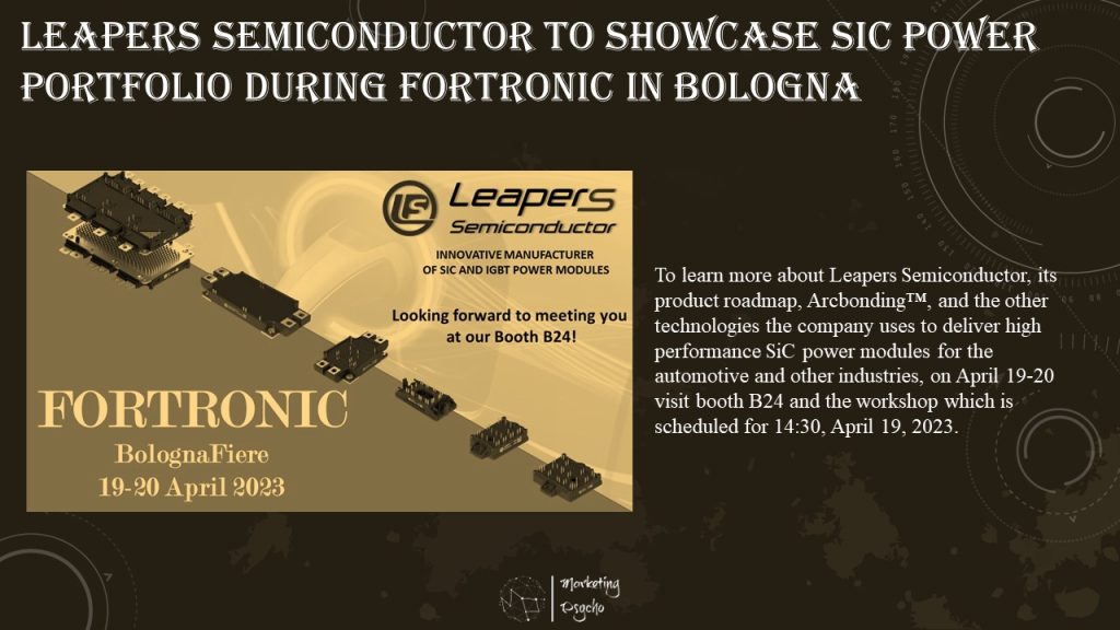
To learn more about Leapers Semiconductor, its product roadmap, Arcbonding™, and the other technologies the company uses to deliver high performance SiC power modules for the automotive and other industries, on April 19-20 visit their booth B24 and the workshop which is scheduled for 14:30, April 19, 2023.
PowerUP Expo Returns in June
Power electronics technologies have undergone a radical transformation following the introduction of wide-bandgap (WBG) devices, such as silicon carbide (SiC) and gallium nitride (GaN). These materials, in fact, have characteristics that make them particularly suitable for applications that operate at high voltages and high switching frequencies. To fully exploit the potential offered by wide-bandgap semiconductors, designers must understand the challenges of these materials.
Power electronics design will continue to focus on reducing the size and complexity of devices while increasing their functionality. The design will increasingly incorporate AI and machine learning algorithms to improve performance, monitor system health, and optimize energy management. Future developments will be integrated not only in automotive, industrial, aerospace markets, but also with IoT technologies to create a more connected and automated energy system.
Semiconductor devices are used to drive motors and control power. As efficiency standards for these applications get better, cost-effective and energy-efficient control solutions, test and measurement solutions, and transducers/sensors make design easier and offer a high level of integration, as well as better safety features and certified isolation capabilities.
Moreover, using energy harvesting techniques and new power semiconductors to make electrical and electronic systems work as well as possible is an important part of engineering.
The PowerUP Expo is a three-day virtual conference and exhibition focusing on power electronics. With an exhibition area, live stage, and messaging center, the PowerUP Expo functions similarly to a live exhibition and conference. This technical conference will include a number of sessions including keynotes, panel discussions, technical presentations, and tutorials on a variety of subject matters, including significant technical trends, market demands, and new application areas. The exhibition area will include virtual booths from top power electronics businesses and a Live Chat facility that allows attendees to communicate with booth staff directly.
PowerUP offers an opportunity for engineers, managers, academics, and students from all over the world to learn the latest technological advances and applications in Power Electronics and to connect with each other in our community. The newest trends and advancements in the field of power electronics, from components to intelligent systems, are discussed by leaders in the industry.
Conference Tracks:
- June 27: Tutorial/Lectures, Panel Discussion & Conference Preview
- June 28: Wide Bandgap Semiconductors and Power Applications
- June 29: Power Conversion and Management Design Trends in low and high power
Detailed agenda can be found at PowerUP Expo.
Subscribe to Power Semiconductors Weekly and watch it on YouTube every Tuesday.
If you prefer a monthly update about the world of power semiconductors delivered to your e-mail address, please, subscribe to Marketing Psycho Power Semiconductors newsletter