Power Semiconductors Weekly Vol. 102
Toshiba’s Lineup Expansion of 150 V N-Channel MOSFETs
Toshiba Electronic Devices & Storage Corporation (“Toshiba”) has expanded the lineup of 150 V N-channel power MOSFETs with new products that adopt the new generation process “U-MOS X-H series.” Products in this series are suitable for the switching power supplies of communication equipment and so forth. They are “TPH1400CQH,” which has a drain-source On-resistance of 14.1 mΩ, and “TPN4800CQH,” which has a drain-source On-resistance of 48 mΩ. Both of them use surface mount packages.
The new products have reduced their drain-source On-resistance compared with the 150 V products using the current generation process U-MOS VIII-H series. In addition, by optimizing the device structure, the products have improved the trade-off between the drain-source On-resistance and output charge, featuring industry-leading[2] low power loss. Moreover, the products have reduced the spike voltage generated between the drain and the source when switching, helping lower the EMI of switching power supplies.
Applications:
- Power supplies for communication equipment
- Switching power supplies (High efficiency DC-DC converters, etc.)
Features:
- Featuring one of the industry-leading low power loss
(Improving the trade-off between the On-resistance and output charge)
- Low On-resistance:
TPH1400CQH RDS(ON)=14.1 mΩ (max) (VGS=10 V)
TPN4800CQH RDS(ON)=48 mΩ (max) (VGS=10 V)
- High channel temperature rating : Tch (max)=175 °C
Microchip Plans to Invest $880 Million to Expand its SiC and Si Capacity in Colorado
Microchip Technology Inc. announced plans to invest $880M to expand its silicon carbide (SiC) and silicon (Si) production capacity at its Colorado Springs, Colo. manufacturing facility over the next several years.
One significant phase of the expansion is to develop and upgrade its 50-acre, 580,000-square-foot Colorado Springs campus for increased SiC manufacturing for use in automotive/E-Mobility, grid infrastructure, green energy, and aerospace and defense applications.
Working in conjunction with the Colorado Springs Chamber & Economic Development Corporation, the City of Colorado Springs and El Paso County also announce that Microchip was approved for state and local incentives of approximately $47M for the expansion.
Colorado Springs Mayor John Suthers said, “We are very pleased Microchip has selected its Colorado Springs facility as the site for such a significant investment and expansion. We estimate this will grow our local economy by approximately $1.4 billion over the next 10 years and create roughly 400 new high-paying jobs for those living in the Pikes Peak Region. Ramping up the production of semiconductors is critical to satisfying growing demand across many industries, and Colorado Springs is proud to be one of the key locations where this effort is taking place.”
U.S. Senator for Colorado Michael Bennet said, “Last year, I helped pass the CHIPS and Science Act to reinvigorate America’s semiconductor industry and bring manufacturing jobs back to America. In Colorado, we’re already seeing the benefits as companies prepare for historic investments from the law. Microchip’s planned expansion in Colorado Springs will not only strengthen our national security, but also expand opportunity with another 400 good-paying jobs.”
U.S. Senator for Colorado John Hickenlooper said, “Thanks to our CHIPS Act and Microchip, we’re bringing manufacturing back to America. Semiconductors are the space race of our time, and Colorado is going to help us win it.”
U.S. Congressman Doug Lamborn said, “It is exciting to have Microchip Technology expanding its footprint and investing in its chip manufacturing facility in Colorado’s 5th Congressional District. As concerns mount over foreign dominance of this critical industry, it is increasingly important that the U.S. achieve domestic production of microchips. I commend the City of Colorado Springs and the Colorado Springs Chamber for their dedication to bringing high-paying, high-quality jobs, and great companies to the Pikes Peak region.”
President and CEO of Microchip Technology Ganesh Moorthy said, “Microchip Colorado Springs has a long history of partnering with the city and state and we applaud their continued support of our efforts to advance the semiconductor industry in the U.S. The CHIPS and Science Act is already making a positive impact on our business through the Investment Tax Credit and we are seeking capacity expansion grants for several of our semiconductor factories, including our Colorado Springs factory. We see a bright future in the region made possible by great partnerships, state and local incentives, and a strong local talented workforce.”
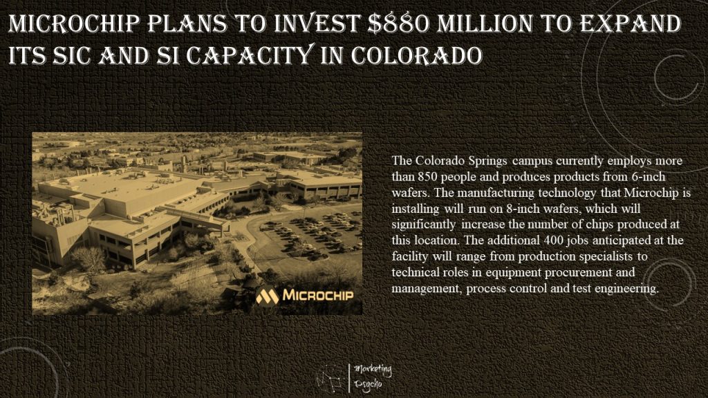
The Colorado Springs campus currently employs more than 850 people and produces products from 6-inch wafers. The manufacturing technology that Microchip is installing will run on 8-inch wafers, which will significantly increase the number of chips produced at this location. The additional 400 jobs anticipated at the facility will range from production specialists to technical roles in equipment procurement and management, process control and test engineering.
“With over two-decades of investment in silicon carbide, Microchip’s portfolio is designed to provide our customers with innovative power solutions,” said Rich Simoncic, senior vice president of Microchip’s Analog businesses. “This campus is an integral part of producing our SiC technology to assure our customers with supply certainty as they transition to SiC solutions.”
“Microchip’s expansion in Colorado Springs and El Paso County puts our region on the map for investment from the CHIPS and Science Act. We are proud to lead Microchip’s expansion project and support the reshoring of these important manufacturing jobs to the Pikes Peak region,” said Johnna Reeder Kleymeyer, President and CEO, Colorado Springs Chamber & Economic Development Corporation.
Infineon Kicks off New Fab in Dresden
Infineon Technologies AG is starting construction of its new plant for analog/mixed-signal technologies and power semiconductors. After extensive analysis, the Infineon Management Board and supervisory bodies gave the green light for the Dresden site. The German Federal Ministry for Economic Affairs and Climate Action (BMWK) has approved an early project launch, meaning that construction can already begin before completion of the inspection of legal subsidy aspects by the European Commission. Subject to the European Commission’s state aid decision and the national grant procedure, the project is to be funded in accordance with the objectives of the European Chips Act. Infineon is seeking public funding of around one billion euros. The company plans to invest a total of approximately five billion euros in the plant, which is set to begin production in 2026. This constitutes the largest single investment in the company’s history.
“We’re picking up the pace by expanding our production capacities in order to leverage the growth opportunities which the megatrends decarbonization and digitalization are offering us,” says Infineon CEO Jochen Hanebeck. “We see structurally growing demand for semiconductors, for example for use in renewable energies, data centers and electro-mobility. By building the 300mm Smart Power Fab in Dresden we are establishing the prerequisites necessary to successfully meet the rising demand for semiconductor solutions.”
Infineon’s investment is an essential contribution to achieving the European Commission’s declared objective of reaching a 20 percent share of global semiconductor production in the EU by 2030. Semiconductor solutions for industrial and automotive applications from the Dresden Fab will help secure value chains in key European industries even better in the future.
In addition, the investment by Infineon strengthens the manufacturing basis for the semiconductors that drive decarbonization and digitalization. Analog/mixed-signal components are used in power supply systems, for example in energy-efficient charging systems, small automotive motor control units, in data centers and in applications for the Internet of Things (IoT). The interaction of power semiconductors and analog/mixed-signal components makes it possible to create particularly energy-efficient and intelligent system solutions.
Expansion of production capacities at the existing Dresden site will let Infineon complete the project quickly and will also generate considerable effects of scale. Construction is set to begin in 2023, with the beginning of manufacturing activities planned for fall 2026. The expansion will create approximately 1,000 highly qualified jobs. When operating at full capacity, the Dresden Fab will let Infineon achieve additional revenues on the order of the investment amount each year.
The plant will be equipped with the latest in environmental technologies and will be among the most environmentally friendly manufacturing facilities of its kind. Thanks to advanced digitalization and automation, Infineon is also setting new manufacturing excellence standards in Dresden. The new plant will be closely linked with the Infineon Villach site as “One Virtual Fab”. This manufacturing complex for power electronics based on highly efficient 300-millimeter technology will increase efficiency levels and give Infineon additional flexibility in order to supply its customers faster.
Texas Instruments Selects Utah for its Next 300-mm Semiconductor Wafer Fab
Texas Instruments Incorporated announced plans to build its next 300-millimeter semiconductor wafer fabrication plant in Lehi, Utah. The new fab will be located next to the company’s existing 300-mm semiconductor wafer fab in Lehi, LFAB. Once completed, TI’s two Lehi fabs will operate as a single fab.
“This new fab is part of our long-term, 300-mm manufacturing roadmap to build the capacity our customers will need for decades to come,” said Haviv Ilan, TI executive vice president and chief operating officer, and incoming president and chief executive officer. “Our decision to build a second fab in Lehi underscores our commitment to Utah and is a testament to the talented team there who will lay the groundwork for another important chapter in TI’s future. With the anticipated growth of semiconductors in electronics, particularly in industrial and automotive, and the passage of the CHIPS and Science Act, there is no better time to further invest in our internal manufacturing capacity.”
The landmark $11 billion investment marks the largest economic investment in Utah history. The Lehi expansion will create approximately 800 additional TI jobs as well as thousands of indirect jobs. TI looks forward to strengthening its partnership with the Alpine School District and will invest $9 million to improve student opportunities and outcomes.
“Companies like Texas Instruments continue to invest in Utah because of our world-class business climate and exceptional workforce,” said Utah Gov. Spencer Cox. “TI’s new semiconductor fab will solidify Utah as a global semiconductor manufacturing hub for generations to come.”

Lehi is an ideal location because of its access to skilled talent, robust existing infrastructure and strong network of community partners. The new fab will manufacture tens of millions of analog and embedded processing chips daily that will go into electronics everywhere.
The fab will be designed to meet one of the Leadership in Energy and Environmental Design (LEED) building rating system’s highest levels of structural efficiency and sustainability: LEED Gold. Plans include recycling water at nearly double the rate of the existing Lehi fab. Advanced 300-mm equipment and processes in Lehi will further reduce waste, water and energy consumption per chip.
Construction of the new fab is expected to begin in the second half of 2023, with production as early as 2026. The cost of the new fab is comprehended in TI’s previously announced capital spending plan to expand manufacturing capacity and will complement TI’s existing 300-mm fabs, which include DMOS6 (Dallas), RFAB1 and RFAB2 (both in Richardson, Texas), and LFAB (Lehi, Utah). TI is also building four new 300-mm wafer fabs in Sherman, Texas.
Amkor Technology and GlobalFoundries to Provide At-scale Semiconductor Test and Assembly Services in Europe
Amkor Technology, Inc., a leading provider of semiconductor packaging and test services, and GlobalFoundries (GF), a global leader in feature-rich semiconductor manufacturing, announced that the two companies have formed a strategic partnership. This new partnership will enable a comprehensive EU/US supply chain from semiconductor wafer production at GF to OSAT (Outsourced Semiconductor Assembly and Test) services at Amkor’s site in Porto, Portugal. GF plans to transfer its 300mm Bump and Sort lines from its Dresden site to Amkor’s Porto operations to establish the first at-scale back-end facility in Europe. GF will maintain ownership of its transferred tools, processes, and IP in Porto. Both partners also plan to collaborate on future development efforts in Portugal.
Today, Amkor is the only high-volume, Tier 1 OSAT in Europe, and GF Dresden is Europe’s largest and most advanced semiconductor manufacturing services company. This partnership enables the first semiconductor manufacturing (foundry) through advanced packaging semiconductor supply chain outside of Asia, creating more European supply chain autonomy for key end markets including automotive.
“This strategic partnership with GF will enhance the advanced semiconductor packaging supply chain in Europe and ramp up competitive capacity to complement what is available in Asia,” said Kevin Engel, Amkor’s Executive Vice President, Business Units. “Amkor’s collaboration with GF enables us to significantly expand manufacturing scale and bring to market additional assembly and test capability to support our European and global customers.”
“GF remains committed to growing our European manufacturing ecosystem to support local and global customers, especially in the Automotive markets. This partnership with Amkor in Portugal will provide much needed services within the EU and expand the US-European semiconductor supply chain,” said Mike Hogan, GlobalFoundries Chief Business Officer.
At this pivotal time in the semiconductor industry, manufacturers and suppliers alike are confronted with political, industrial, technological, and financial disruptions. Amkor’s global support and local presence combined with GF’s tools and processes will enable the Porto site to help the European Union pursue its goals of ensuring supply chain stability and delivering the next-generation automotive and other critical chip solutions.
ECPE SiC & GaN User Forum: Potential of Wide Bandgap Semiconductors in Power Electronic Applications
Since more than 16 years the biannual ECPE Wide Bandgap User Forum has explained the background and given advise and support to design-in SiC and GaN semiconductor devices in power electronic systems. Major progress has been achieved in this period, with today a multitude of SiC diodes and MOSFETs and as well GaN HEMTs being available and used in series products.
For those, special aspects gain importance, such as robustness or qualification when exposed to demanding mission profiles. On the other hand, still more basic research and development work is dedicated to special devices made by SiC, GaN and other wide bandgap materials including their potential applications.
These actual topics will be addressed during the upcoming 10th ECPE Wide Bandgap User Forum.
The programme will start with an overview on the status and trends in WBG Power Electronics. Then, the 1st day is dedicated to the use of GaN HEMTs in different systems and applications. Recent developments e.g., on bidirectional HEMTs, multi-channel tri-gate devices and vertical GaN devices will also be presented and discussed.
The 2nd workshop day will concentrate on SiC device applications. Further, an outlook on promising ultra-wide bandgap (UWBG) materials and devices will be given. The workshop will be closed with a panel discussion addressing the topics of WBG device maturity, robustness, and reliability.
International renowned experts are being invited to give an overview and to in depth explain their research and development work in technical presentations. Besides, the ECPE Wide Bandgap User Forum offers a platform for all participants to share experience and ideas.
- Date: 28/03/2023 – 29/03/2023
- Location: Erding / Munich, Germany
- Registration Deadline: 22 March 2023
Subscribe to Power Semiconductors Weekly and watch it on YouTube every Tuesday.
If you prefer a monthly update about the world of power semiconductors delivered to your e-mail address, please, subscribe to Marketing Psycho Power Semiconductors newsletter