Power Semiconductors Weekly Vol. 101
Infineon QDPAK and DDPAK Packages Registered as JEDEC Standard for High-Power Applications
The trends toward higher power density and cost optimization dominate the development goals of efficient high-power applications that create substantial value for segments such as electromobility. To push these boundaries, Infineon Technologies AG announced it has successfully registered its QDPAK and DDPAK top-side cooling (TSC) packages, which are ideal for high-voltage MOSFETs as a JEDEC standard. This registration further solidifies Infineon’s goal to help establish a broad adoption of TSC in new designs with one standard package design and footprint. Additionally, this provides flexibility and comfort to OEM manufacturers to differentiate their products in the market and take power density to the next level to support various applications.
“As a solutions provider, Infineon continues to influence the semiconductor industry through innovative packaging technologies and manufacturing processes,” said Ralf Otremba, Lead Principal Engineer for High Voltage Packaging, Infineon. “Our advanced top-side cooled packages bring significant advantages to the device and system levels to fulfill the challenging demands of cutting-edge high-power designs. Package outline standardization will help ease one of the main design concerns of OEMs for high-voltage applications by securing pin-to-pin compatibility across vendors.”
For more than 50 years, the JEDEC organization has been the global leader in developing open standards and publications for the microelectronics industry for a broad range of technologies, including package outlines. JEDEC has been widely accepting semiconductor packages such as the TO220 and TO247 through-hole devices (THD) – devices that have been prominently used over the past decades and are still an option in new onboard charger (OBC) designs, high voltage (HV) and low voltage (LV) DC-DC converters.
The registration of QDPAK and DDPAK surface-mounted (SMD) TSC package designs signals a new era for package outlines ushering a wide market adoption of the TSC technology as a replacement for TO247 and TO220, respectively. With the benefits of this technology, this new JEDEC package family registration, according to the MO-354 standard, serves as a key enabler for the transition of high-voltage industrial and automotive applications to top-side cooled designs in next-generation platforms.
To facilitate design transition for customers from the TO220 and TO247 THD devices, Infineon has designed QDPAK and DDPAK SMD devices to deliver equivalent thermal capabilities with improved electrical performance. Based on a standard height of 2.3 mm for QDPAK and DDPAK SMD TSC package for HV and LV devices, developers are now able to design complete applications such as OBC and DC-DC conversion with all SMD TSC devices measuring the same height. Compared to existing solutions that require a 3D cooling system, this facilitates designs and reduces system cost for cooling.
Additionally, TSC packaging offers up to 35 percent lower thermal resistance than standard bottom-side cooling (BSC). By enabling the use of both PCB sides, TSC packages offer better board space utilization and at least two times more power density. The thermal management of the packages is also improved by thermal decoupling from the substrate since the thermal resistance of the leads is much higher compared to the exposed package top side. Because of the improved thermal performance, stacking different boards is not necessary. Rather than combining both FR4 and IMS, a single FR4 is enough for all components and also requires fewer connectors. These features deliver an overall bill of materials (BOM), which ultimately reduces overall system cost.
In addition to improved thermal and power capabilities, TSC technology also offers an optimized power loop design for increased reliability. This is possible by the placement of the drivers, which can be placed very close to the power switch. The low stray inductance of the driver switch loop, reduces the loop parasitics and leads to less ringing on the gate, higher performance and a smaller risk of failures.
Polar Semiconductor Investment and Expansion
Allegro MicroSystems, Inc. announced that Polar Semiconductor, a company jointly-owned by Allegro and Sanken Electric Co., Ltd. (“Sanken”), and one of Allegro’s primary suppliers of 200 millimeter wafers, is expected to receive a $150 million equity investment from an affiliate of One Equity Partners to expand 200 millimeter sensor and high voltage power wafer capacity at its fabrication facility in Bloomington, Minnesota. In conjunction with this investment, Polar is also pursuing U.S. CHIPS Act funding to further invest in its capacity and cost leadership initiatives to supply sensor and high voltage power wafers for critical automotive and industrial applications.
This investment is expected to provide Allegro with expanded U.S.-based capacity to support customers for years to come. “We appreciate our longstanding relationship with Polar and look forward to continued partnership to support anticipated growing customer demand,” said Vineet Nargolwala, Allegro Microsystems President, and CEO.
The transaction is expected to close in the first quarter of Allegro’s 2024 fiscal year.
Pan-European Research Initiative PowerizeD for Intelligent Power Electronics Launched
Over 100 representatives from 39 companies and 23 research institutions held a meeting in Munich at the Campeon, headquarters of Infineon Technologies AG, for the kick-off of the European research initiative PowerizeD. They are focusing on intelligence in power electronics and thus want to contribute to the decarbonization of European society and the protection of our climate. PowerizeD is to take the sustainability and resilience of the European energy chain, from generation to application, to a new level and strengthen Europe’s technological sovereignty. 62 research partners from 13 European countries are involved in the major European project with an overall volume of 72 million euros. PowerizeD addresses a new level of technology and relies increasingly on the digitalization of power applications. Infineon Technologies AG initiated the project, is an active participant with several corporate divisions and is also the overall project coordinator.
“We have to make highly efficient use of energy if we are to achieve net-zero climate protection goals. Digitalization can help here as a highly decisive lever for more energy efficiency,” says Constanze Hufenbecher, Infineon Chief Digital Transformation Officer. “We are pleased to be able to combine our strengths with the strengths of so many excellent partners from research and business to jointly make the ambitious European research initiative PowerizeD a success.”
“Power electronics is key to the energy transformation and is used anywhere and everywhere that electricity is generated, transferred and used efficiently,” says Dr. Rutger Wijburg, Chief Operations Officer at Infineon. “The broad spectrum of power electronics applications makes it very important that we collaborate with partners across the boundaries of corporate entities and organizations to jointly advance Europe as innovation engine.”
The project partners are focusing on applications from the fields Energy and Mobility. 17 demonstrator paths are concerned among other things with improvement of drives for the rail industry, charging systems for the automotive industry, liquid batteries for the energy industry as well as drives for the manufacturing industries. The research partners will take an interdisciplinary approach with topics including modeling and Digital Twin, Federated Learning as well as reliability and sustainability.
The newly developed key technologies are to be realized and demonstrated in concrete form and are to be evaluated in terms of a large number of universally applicable results. The immediate project objectives include:
- Reduction of power loss in power conversion by 25 percent
- Extension of the service lives of devices and systems by 30 percent
- Reduction of chip size by at least 10 percent
- Shortening development times by a challenging 50 percent
Technologically speaking, PowerizeD is to increase the degree of mechanical and electrical integration of control, driver and switching functionalities in components and to advance the integrated optimization of all power switch functionalities, independent of the semiconductor material used. New switching topologies and advanced control strategies involving the application of Artificial Intelligence are to improve efficient, robust, and reliable operations even further.
The European Union is funding PowerizeD with approximately 18 million euros as part of the joint program for digital key technologies (Key Digital Technologies Joint Undertaking, KDT JU) in its Digital Agenda. The amount will be matched by funding from the national governments of the respective countries involved. The subsidies from Germany are being provided by the German Federal Ministry of Education and Research. A summary of all the project partners and supporting organizations is available on the project web site. The project will have a three-year duration and is expected to end in December 2025.
Further information on the project and the project partners can be found at the following web site: www.powerized.eu.
20 years of LFPAK Technology
Up until relatively recently, the packaging of power semiconductors was not high on the list of priorities when designing products. However, the continuing need to fit more power into smaller footprints has meant that situation has changed, and the specifications of the packaging have become almost as important as the design of the silicon inside. High power density means that the packaging has a more important role in taking heat away from the die.
Wire-bonding was initially the preferred method of attaching the die to the outside world, but as density and currents increased, a single wire could no longer provide an efficient link and that was detrimental to the operation of the device. Wires were then made thicker to handle more current, and additional wires were added, but that didn’t completely solve the problem and the expected gains from new designs were still not being realized. Wires also expand and contract with heat, and each time that happens it places a strain on the bond and lowers the lifetime of the device.
In 2002, Nexperia engineers, while still part of Dutch multinational Philips, developed a new concept that eliminated the need for wires to be bonded to the die. Instead, they used large copper clip attached to the source metallization on the topside of the die to connect it to the outside circuit. Gull wing pins were also developed that could efficiently carry higher currents, while still being flexible enough to cater for heat expansion and contraction without damaging the connection to the die or board, and therefore increasing reliability. The new LFPAK package significantly lowered both the thermal and electrical on-resistance of the device, outperforming traditional Power-SO8 packages.
Chris Boyce, Senior Director, Marketing & Product Group, BG MOS Discretes at Nexperia explains how revolutionary the package was at the time, “It’s easy to forget how much has changed in 20 years. Some of the innovations now seem obvious and have been replicated a number of different ways. However, at the time it was pioneering, and the LFPAK devices gained rapid market acceptance, with initial deployments in engine control systems, braking, ABS products and power steering”.
Boyce continues by describing how the LFPAK has increased reliability, “The gull wing pins act like a shock absorber and give excellent board level reliability, and the evidence of that is clear now that LFPAK devices have been in the field for 20 years. All of the theory has has played out in practice over the long term”.
Semiconductor technology has evolved over the last two decades and Nexperia engineers have continued to refine and improve the LFPAK concept to cope with its increasing demands. Each iteration has improved LFPAK’s performance with lower RDS(on), lighter-weight clips, reduced gate pads and thinner wafers.
Today, around 90% of the Nexperia product range is LFPAK-based, with more than 400 devices across 7 distinct design variants. The original LFPAK56, (named after its dimensions – 5 mm x 6 mm) was soon followed by the LFPAK33, and the LFPAK88, delivering the benefits of the latest device package technology in a wide range of voltage and current ratings. Today a single MOSFET in LFPAK88 boasts an RDS(on) of just 0.55 mΩ handling a maximum current of 500 A.
Dual LFPAK devices are also available, containing two individual MOSFET dies in one package, offering additional space-saving. Nexperia has also produced an additional variant of the LFPAK56D containing a series of MOSFETs in half-bridge configuration, for space constrained motor applications. Some of the latest innovation in LFPAK-type packaging has come from the need to integrate wide bandgap materials. CCPAK is a copper clip cascode GaN HEMT package that brings all the benefits of copper clip, such as thermal performance and board level reliability to power GaN FETs.
Almost 10 billion LFPAK MOSFETs have been shipped since production began, with 1.7 billion in 2021 alone.
Boyce concludes by looking to the future, “Although it started with a 5 mm x 6 mm device twenty years ago, we’ve expanded the portfolio significantly over the years. Now, we have the CCPAK 1212, a new 12 mm x 12 mm package that we use for GaN devices. It’s non trivial to make them work and be able to produce them in in huge volumes, and its taken a lot of learning and experience from working with LFPAK technology to accomplish that. There will be future generations of packages that will also build on the learning of the team, which includes 12 of the original LFPAK creators. We are not done yet, and hopefully we will come back in another 10 years with an update”.
PCIM Asia Conference 2023 Call for Papers Open
PCIM Asia 2023 and the PCIM Asia Conference will once again offer an in-depth exploration of the latest developments in the power electronics industry, with a range of interactive seminars, workshops, and networking opportunities. Attendees can expect to gain valuable insights into the latest technology trends, market opportunities, and best practices from industry experts.
Prof. Dr. Leo Lorenz, Chairman of the PCIM Advisory Board shared his thoughts on the upcoming edition: “PCIM Asia 2023 is set to remain as one of the most important events of the year for the power electronics and intelligent motion industry in the region. It will once again provide a platform for industry professionals to come together to discuss the latest technologies, trends, and developments in the field, and to build relationships that will last far beyond the event.”
The “Electrification of Transportation Systems” will be highlighted at the 2023 conference alongside other key topics including:
- Advanced Power Semiconductors
- Packaging and Reliability
- Passive Components and Integration
- AC/DC Converter
- DC/DC Converter
- Digital Power Conversion
- Motor Drive & Motion Control
- High Frequency Power Electronic Converters and Inverters
- Automotive Power Electronics
- System Reliability
- Power Quality Solutions
- Smart Grid Power Electronics
- Power Electronics in Transmission Systems
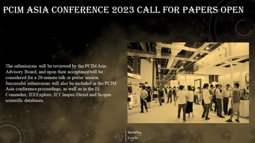
The submissions will be reviewed by the PCIM Asia Advisory Board, and upon their acceptance will be considered for a 20-minute talk or poster session. Successful submissions will also be included in the PCIM Asia conference proceedings, as well as in the Ei Comendex, IEEExplore, IET Inspec-Direct and Scopus scientific databases.
As always, there will be three awards honoring the most outstanding achievements and contributions of researchers, with all winners receiving an attractive prize. Awards include “The Best Paper Award” for the best overall submission, “The Young Engineer Award”, which recognizes an engineer under the age of 35 for an outstanding paper and “The University Scientist Award” for universities best promoting the development of the power electronics industry.
PowerAmerica Webinar: Bidirectional SiC and GaN Switch Technology
There are numerous mass volume power applications where it is necessary to control the flow of bidirectional power, including electric vehicles (vehicle to grid, vehicle to home, and vehicle to vehicle), distributed and grid-tie power systems using regenerated energy and/or energy storage components, and solid-state circuit breaker protection.
Silicon carbide (SiC) and gallium nitride (GaN) based bidirectional power switches can enable these applications with their compelling advantages of high efficiency, high blocking voltage capability, and low system weight and volume. In particular, monolithic switches that allow for bidirectional symmetric conduction and voltage blocking with a chip area close to that of a similarly rated unidirectional switch are ideally suited to fuel a revolution in power electronics technology.
Today, monolithic bidirectional (MBD) power semiconductor switches are not commercially available. Instead, back-to-back (anti-series) connection schemes of unidirectional power MOSFETs or IGBTs are typically used, resulting in a 4X penalty in chip area and high cost. However, various types of SiC and GaN bidirectional concepts are being investigated including bonded-wafer bidirectional IGBTs, monolithic dual-gate bidirectional GaN switches, and monolithic back-to-back connected SiC MOSFETs and JFETs.
In this webinar, the semiconductor technology of SiC and GaN bidirectional switches will be reviewed including their operating principles, and their lateral and vertical geometry configurations. The performance advantages of MBD switches will be highlighted. Promising MBD devices reported to date will be analyzed, and the key bidirectional switch applications of solid-state circuit breakers and current-source-inverters will be discussed. As SiC and GaN devices approach mass commercialization propelled by insertion in electric vehicles and consumer electronics, respectively, fabrication of SiC/GaN MBD switches is becoming economically viable enabling their wide adoption in key volume applications.
In this PowerAmerica webinar of the SiC series, you’ll learn:
- Advantages of bidirectional SiC and GaN switch technology
- Performance advantages of monolithic bidirectional switches
- Date: February 21, 2023
- Time: 1 PM EST
Subscribe to Power Semiconductors Weekly and watch it on YouTube every Tuesday.
If you prefer a monthly update about the world of power semiconductors delivered to your e-mail address, please, subscribe to Marketing Psycho Power Semiconductors newsletter