Power Semiconductors Weekly Vol. 92
Vishay Presents Three Phase Bridge Power Modules in the Compact MTC Package
Vishay Intertechnology, Inc. introduced three new series of 130 A to 300 A three phase bridge power modules in the ultra-compact MTC package that deliver reliable operation for heavy-duty industrial applications. The Vishay Semiconductors devices are produced at the company’s assembly site in Mumbai, India, and are thus excluded from extra tariffs.
The 130 A VS-131MT…C, 160 A VS-161MT…C, and 300 A VS-301MT…C series are optimized for line-frequency input rectification in welding machines, switch mode power supplies, plasma cutting, battery chargers, and motor control. The encapsulated devices offer a rugged design for these applications, while their highly conductive MTC package provides excellent thermal behavior.
Offering a simple, screw-mount connection to reduce assembly time, each power module series released is available with blocking voltages of 1600 V and 1800 V. The devices offer 3600 VRMS isolation voltage, low forward voltage down to 1.54 V, and low junction to case thermal resistance down to 0.038 °C/W. Designed and qualified for industrial-level applications, the RoHS-compliant solutions are UL-approved, file E78996.
Toshiba Develops SiC MOSFET with Embedded Schottky Barrier Diode
Toshiba Electronic Devices & Storage Corporation and Toshiba Corporation (collectively “Toshiba”) have developed a SiC metal oxide semiconductor field effect transistor (MOSFET) that arranges embedded Schottky barrier diodes (SBD) in a check pattern (check-pattern embedded SBD) to realize both low on-resistance and high reliability. Toshiba has confirmed that the design secures an approximately 20% reduction in on-resistance (RonA) against its current SiC MOSFET, with no loss of reliability.
Power devices are essential components for managing electric energy and reducing power loss in all kinds of electronic equipment, and for achieving a carbon neutral society. SiC is widely seen as the next generation material for the devices, as it delivers higher voltages and lower losses than silicon. While use of SiC now largely limited to inverters for trains, wider application is on the horizon, in areas including vehicle electrification and the miniaturization of industrial equipment. However, there is a problem that must first be overcome: bipolar conduction in the body diode during reverse operation of SiC MOSFET is harmful because it degrades on-resistance.
Toshiba Electronic Devices & Storage Corporation developed a device structure that embeds SBDs into the MOSFET to inactivate body diodes, but it found that replacing the MOSFET channel with an embedded SBD lowers channel density and increases RonA. This trade-off has now been resolved with a new embedded SBD structure, and Toshiba has confirmed that it dramatically improves performance characteristics.

Toshiba has improved both conduction loss in its SBD-embedded SiC MOSFET, and achieved good diode conductivity, by deploying a check-pattern SBD distribution. Evaluation of the on-side current characteristics of 1.2kV-class-SBD-embedded MOSFETs with the optimized design confirmed that using the check design to position the embedded-SBDs close to the body diodes effectively limits bipolar conduction of the parasitic diodes, while the unipolar current limit of reverse conduction is double that realized by the current striped SBD pattern design for the same SBD area consumption. RonA was found to be approximately 20% lower, at 2.7mΩ・cm2.
This confirmed improvement in the trade-off is essential if SiC MOSFETs are to be used in inverters for motor drive applications. Toshiba is continuing to carry out evaluations toward improving dynamic characteristics and reliability, and to develop attractive, high performance power semiconductors that contribute to carbon neutrality.
Details of the achievement were reported at the 68th Annual IEEE International Electron Devices Meeting, an international power semiconductor conference held in San Francisco, USA, on December 3 to 7.
Vincotech Updates MiniSkiiP® Product Line
The asymmetric bridge conversion represents the best approach to powering low-cost, efficient and robust switched reluctance motors (SRM). Vincotech’s new 1200 V PIM family based on asymmetric bridge topology supports the design with a flexible and cost-effective solution.
The updates product family of MiniSKiiP® include:
- MiniSKiiP® PIM 3 (35 A)
- MiniSKiiP® PIM 3 (50 A)
- MiniSKiiP® PIM 2
Main benefits:
- Highly efficient asymmetric bridge topology suitable for SRM
- Latest generation chipsets with 15 A, 35 A and 50 A nominal current for wide power range offer
- Integrated thermal sensor simplifies temperature measurement
Soitec Breaks Ground on Singapore Fab Extension
Soitec broke ground on the construction of its wafer fab extension at Singapore’s Pasir Ris Wafer Fab Park. The ceremony was held in the presence of Low Yen Ling, Singapore’s Minister of State for Trade and Industry, and Her Excellency, Minh-di Tang, Ambassador of France to Singapore.
The fab extension will be dedicated to the production of 300mm SOI wafers, which are used to produce chips for smartphones, particularly in 5G communications, as well as vehicles and smart devices. Upon its completion in 2024, the extension will add 45,000 square meters of clean room and office space and enable Soitec to double its annual production capacity in Singapore to around two million 300mm SOI wafers.
The extension has been designed to support Soitec’s commitments to an energy-efficient use of resources and make the new facility a sustainable, state-of-the-art working environment. Soitec aims to double its workforce in Pasir Ris to more than 600 by 2026. In parallel to this extension, Soitec is also expanding its technology presence in Singapore with the operational start of its characterization Lab within Soitec’s Singapore Technology Center.
Soitec’s addressable market for engineered wafers is expected to expand more than twofold by 2026, from around 3.5 million to over 7 million wafers, fueled by increasing 5G adoption, vehicle electrification and automation as well as burgeoning demand for connected, intelligent devices.
The extension of Pasir Ris in Singapore complements Soitec’s investments in France and is part of its strategy to meet the increasing demand by ramping up its global annual production capacity to around 4.5 million wafers by fiscal year 2026. This includes a wide range of specialized energy-efficient wafers, using different materials (Silicon-on-Insulator, Gallium Nitride, Piezoelectric-on-Insulator and Silicon Carbide) and to serve different markets. Soitec’s investments in Singapore and France are part of a five-year €1.1bn capital expenditure program announced in June 2021.
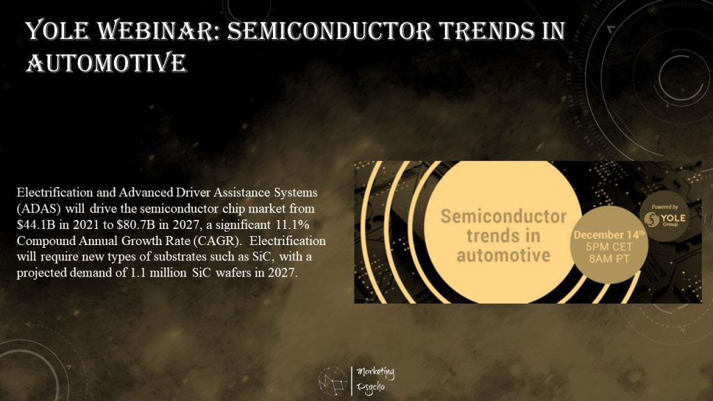
Yole Webinar: Semiconductor Trends in Automotive
Electrification and Advanced Driver Assistance Systems (ADAS) will drive the semiconductor chip market from $44.1B in 2021 to $80.7B in 2027, a significant 11.1% Compound Annual Growth Rate (CAGR). Electrification will require new types of substrates such as SiC, with a projected demand of 1.1 million SiC wafers in 2027. ADAS will use MicroController Units (MCUs) with cutting-edge silicon technology nodes as small as 16nm/10nm. Level 4 and 5 vehicle autonomy will drive demand for Dynamic Random Access Memory (DRAM) and computing power.
These big technological changes also deeply affect the current automotive supply chain. For electrification, vertical integration is becoming popular among car-making OEMs. It can be accomplished in multiple ways. One is full integration down to component level. One is system integration and subcontracting build-to-print parts. Another is strategic cooperation and direct investments with key component suppliers. Players in the conventional automotive supply chain need to thoroughly examine their positions and transform to retain a competitive portfolio through joint ventures, mergers and acquisitions, new investments, and divestments.
Although semiconductors are critical to the ongoing disruptive transition in the automotive industry, most players, whether OEMs or tier-1 suppliers, do not yet have a well-defined strategy for semiconductors. Specific expertise in semiconductor technology and the supply chain, both internal and external, is urgently needed to prepare for the future.
This Yole webcast will present these different topics as well as market data.
- Date: December 14, 2022
- Time: 5 PM CET
NexGen Power Systems Webinar: NexGen Vertical GaN™ Deep Dive: The Future of Power Semiconductors
The world is looking beyond silicon for the next generation of power electronics. NexGen Vertical GaN™ is the world’s first GaN-on-GaN power semiconductor, unlocking the full potential of Gallium Nitride (GaN).
It is the only wide band gap power semiconductor that provides high-voltage capabilities up to 4kV, switching frequencies up to 10MHz, and avalanche and short-circuit robustness. This makes it an ideal power semiconductor for applications for a broad array of applications, including LED Lighting and Computing to Data Centers, Industrial Automation and Electric Vehicles.
NexGen is reinventing power electronics by leveraging this breakthrough technology in a scalable, software-configurable power platform to build the world’s smallest, lightest, and most efficient power systems.
Join this NexGen webinar to learn more about:
- NexGen Vertical GaN™ technology architecture and benefits:
- High Switching Frequency
- High Breakdown Voltage
- High Reliability
- Power Systems based on NexGen Vertical GaN™
- How to get started with NexGen
- Date: December 15, 2022
- Time: 12 PM ET
Subscribe to Power Semiconductors Weekly and watch it on YouTube every Tuesday.
If you prefer a monthly update about the world of power semiconductors delivered to your e-mail address, please, subscribe to Marketing Psycho Power Semiconductors newsletter.