Power Semiconductors Weekly Vol. 80
Toshiba’s New SiC MOSFETs Delivers Low On-Resistance and Significantly Reduced Switching Loss
Toshiba Electronic Devices & Storage Corporation (“Toshiba”) has developed silicon carbide (SiC) MOSFETs with low on-resistance and significantly reduced switching loss—about 20% lower than in its second-generation SiC MOSFETs.
Power devices are essential components for managing and reducing power consumption in all kinds of electronic equipment, and for achieving a carbon neutral society. SiC is widely seen as the next generation material for power devices, as it delivers higher voltages and lower losses than silicon. While SiC power devices are now mainly utilized in inverters for trains, wider application is on the horizon, in vehicle electrification and the miniaturization of industrial equipment. However, the adoption and market growth of SiC devices have been held back by reliability issues.
Toshiba has solved this problem by adopting a structure in which a Schottky Barrier Diode (SBD) is placed in parallel with the PN diode inside the SiC MOSFET of the second-generation product. However, this created a new problem, whereby the performance of the MOSFET deteriorates when it includes an SBD cell that does not operate as a MOSFET. Specifically, there is an increase in the on-resistance per unit area (RonA) and in the performance index that indicates the on-resistance and high speed (Ron*Qgd). A further problem was a higher unit cost from increasing the chip area to reduce on-resistance (Ron).
Toshiba has now developed a device structure that reduces RonA while including an SBD. Spread resistance (Rspread) is reduced and the SBD current is increased by injecting nitrogen into the bottom of the wide p-type diffusion region (p-well) of the SiC MOSFET. Toshiba also reduced the JFET region and injected nitrogen to reduce feedback capacitance and JFET resistance. As a result, feedback capacitance was reduced without increasing RonA. Toshiba prototyped and confirmed that this device structure reduces RonA by 43%, Ron*Qgd by 80%, and switching loss (from switching on and off) by about 20%, compared to its second-generation products. Stable operation without fluctuation of RonA was also secured by optimized positioning of the SBD.
Toshiba plans to start mass production of third generation SiC MOSFETs with the new technology in late August this year.
UnitedSiC (now Qorvo®) Extends Highest Performance, Most Efficient 750V SiC FET Portfolio for Power Designs
Qorvo® announced seven 750V silicon carbide (SiC) FETs in the surface mount D2PAK-7L package. With this package option, Qorvo’s SiC FETs are tailored for the rapidly growing applications of onboard chargers, soft-switched DC/DC converters, battery charging (fast DC and industrial) and IT/server power supplies. They deliver an optimal solution for high-power applications that require maximum efficiency, low conduction losses and excellent cost effectiveness in a thermally enhanced package.

Highlighted by the industry’s lowest RDS(on) of 9 milliohms (mohms) at 650/750V, the Gen 4 UJ4C/SC series is rated at 9, 11, 18, 23, 33, 44 and 60 mohms. This wide selection provides engineers with more device options, enabling greater flexibility to achieve an optimum cost/efficiency balance while maintaining generous design margins and circuit robustness. Leveraging a unique cascode SiC FET technology in which a normally-on SiC JFET is co-packaged with a Si MOSFET to produce a normally-off SiC FET, these devices deliver a best-in-class RDS x A figure of merit, resulting in the lowest conduction losses in a small die.
Anup Bhalla, chief engineer at UnitedSiC (now Qorvo), said, “The D2PAK-7L package reduces inductance from compact internal connection loops which ─ along with the included Kelvin source connection ─ results in low switching loss, enabling higher frequency operation and improved system power density. These devices also feature silver-sinter die attach, resulting in very low thermal resistance for maximum heat extraction on standard PCBs as well as IMS substrates with liquid cooling.”
flowBOOST Dual and Triple Boosters for 1500 V Solar Inverters
Making the right design choices is critical to a product’s market success. Vincotech‘s dual and triple boost modules for 1500 V solar inverters offer designers even more options on the path to that success. Featuring a combination of Si and SiC components, Vincotech’s extensive range of symmetric and flying capacitor boosters are optimized for cost and performance. The right engineering decision has never been easier to make.
Available in low inductance flow 1, flow 2 and flow S3 housings and tailored for 1500 V solar inverters, these modules are your first and best choice for the latest generation of high-power solar inverter systems.
Main Benefits:
- Complete family including dual and triple symmetric and flying capacitor topologies
- Up to 40 kW per leg
- Optional bypass and auxiliary diodes
- Available in flow 1, flow 2 and flow S3 housings
- Solder or Press-fit pins and pre-applied TIM to help reduce production cost
LPE and A*Star’s Institute Of Microelectronics To Develop High Quality 200mm SiC and Specialty Epitaxy Processes
LPE and the Institute of Microelectronics (IME) at the Agency for Science, Technology and Research (A*STAR) have announced a research collaboration to develop high quality 200mm silicon carbide (SiC) and specialty epitaxy processes including enhanced growth rates with improved uniformity. This will be done through experimental activities supported by simulation studies.
Under the collaboration, the parties will leverage LPE’s knowledge in SiC chemical vapour deposition (CVD) reactor technology and SiC epitaxial growth, plus IME’s research capabilities and facilities, 200mm SiC pilot process integration line, and cutting-edge material characterization equipment. The aim is to create 200mm epitaxy processes with enhanced growth rate and uniformities, and reduced killer defect densities.
The 200mm SiC pilot line is being established by A*STAR’s IME to validate 200mm manufacturing processes and tools on a pilot scale before transitioning to 200mm high-volume manufacturing. This collaboration will be part of IME’s plans for establishing a 200mm SiC innovation programme.
SiC epitaxy is one of the essential process steps for 200mm device processing of the upcoming 200mm SiC pilot line. The manufacturing industry is projected to move towards using a unique single-wafer chamber SiC epitaxy tool. LPE, which contributes their tools into the innovation programme, is geared towards quicker industrial adoption.
For this collaboration, both parties will work on the development of high quality 200mm SiC and specialty epitaxy processes, including the following areas:
- Validation of LPE PE1O8 SiC epitaxy reactor for 150mm / 200mm wafers
- Enhancement of 200mm SiC epilayer uniformity
- Development of 200mm SiC epitaxy processes with increased growth rates
- Development of specialty SiC epitaxy processes on 200mm SiC wafers
“All of us at LPE are very excited about the collaboration with A*STAR’s IME which will result in extraordinary market expansion of 200mm SiC based devices. As SiC power modules become pervasive, a more efficient use of electrical power will make a sustainable growth possible,” said Franco Preti, CEO at LPE.
“We look forward to this joint research between A*STAR’s Institute of Microelectronics and LPE to develop high quality 200mm SiC and specialty epitaxy processes,” said Mr Terence Gan, Executive Director, A*STAR’s IME. “The success of this collaboration will benefit the SiC manufacturing ecosystem and accelerate the adoption of high performance SiC power modules across various applications such as electric vehicles and charging points,” he added.
Japan’s Denso Pushes EV Efficiency with New Power Semiconductors
Top Japanese auto parts supplier Denso has developed a power semiconductor device for electrified vehicles that can reduce energy loss by 20%, seeking a bigger role in the technologies that make electric vehicles stand apart in a crowded market.
Power chips, along with analog semiconductor devices that monitor battery health, are vital to electric vehicle performance. Denso is stepping up in-house development and production of these components rather than outsourcing design and manufacturing, as it does with other automotive chips.
Denso is working to make its silicon-based power chips more cost competitive. Its new RC-IGBT, which integrates a diode into a type of power semiconductor device known as an insulated gate bipolar transistor, is around 30% smaller than existing products on the market, while also cutting down on power losses.
In April, Denso announced a partnership with Taiwanese contract chipmaker United Microelectronics Corp. to produce power semiconductors on 300-millimeter wafers at UMC’s fabrication facility in Japan, starting as early as next year.
The larger wafers enable more efficient production, which Denso sees lowering costs by around 20% compared with standard 200-mm wafers.
The Toyota Motor-affiliated supplier is also working on next-generation power semiconductors made with silicon carbide, which lose less energy and can cut electricity consumption by around 10%. Tesla is leading the way in the use of SiC-based power modules in EVs.
But production of the necessary wafers, which involves crystallizing powdered materials at a high temperature, remains a challenge. Denso is developing a new method that uses heated gases, aiming to make the process 15 times faster and 30% cheaper.
Denso developed its own equipment for this process. It will consider partnering with other manufacturers as it prepares for mass-production. EVs require high-voltage, high-capacity batteries that need to be monitored down to each cell. Denso says it has developed an analog chip that can track 25 cells, twice as many as its competitors.
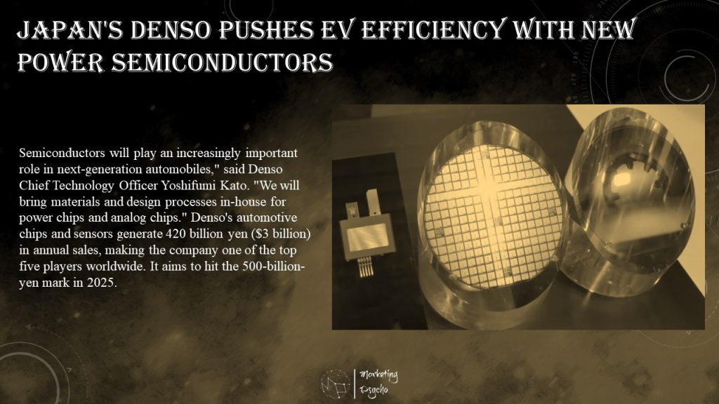
Semiconductors will play an increasingly important role in next-generation automobiles,” said Denso Chief Technology Officer Yoshifumi Kato. “We will bring materials and design processes in-house for power chips and analog chips.” Denso’s automotive chips and sensors generate 420 billion yen ($3 billion) in annual sales, making the company one of the top five players worldwide. It aims to hit the 500-billion-yen mark in 2025. The company made 160 billion yen in capital investments in chip-related fields between fiscal 2019 and fiscal 2021. “We will continue to increase” investment, Kato said
Infineon Webinar: Hybrid and Electric Solutions for Commercial Vehicles
Targets set in emissions standards in many parts of the world to reduce greenhouse gas and pollutant emissions from transport have brought electric propulsion to the fore in recent years and is revolutionizing transport. In addition to passenger cars, more and more commercial vehicles such as trucks, buses and vans, as well as agricultural and construction vehicles, are being powered electrically. This makes them more environmentally friendly, quieter and more efficient than their predecessors with combustion engines.
In this Infineon webinar, you will get an overview of power modules that offer electrical performance and highest reliability without limiting the design flexibility. Infineon’s cutting-edge power modules come in different product families, configurations and current ratings.
Key Take-Aways
- Learn how Infineon responds to the trends and challenges in the electrification of the CAV market
- Explore Infineon’s power modules for hybrid and electric solutions as well as our sense and actuate portfolio
- Examine how Infineon serves applications with increasing demand of semiconductors in the industry
- Date: August 09, 2022
- Time: 3 PM CEST
- Duration: 1 hour
Subscribe to Power Semiconductors Weekly and watch it on YouTube every Tuesday.
If you prefer a monthly update about the world of power semiconductors delivered to your e-mail address, please, subscribe to Marketing Psycho Power Semiconductors newsletter.