Power Semiconductors Weekly Vol. 70
Sensitron and EPC Collaborate to Introduce a High-Power Density 350 V GaN Intelligent Power Module
Reducing size and cost were key concerns of Sensitron when designing their latest generation GaN power modules. By replacing traditional silicon FETs with EPC’s 350 V, EPC2050 GaN FET, Sensitron was able to reduce the size of their solution by 60% while also improving the module’s already excellent junction-to-case thermal conduction. The SPG025N035P1B from Sensitron is a high-power density 350 V, 20 A GaN half bridge with an integrated gate drive, optimized for stray inductance and switching performance at 500 khz. Rated at 20 A, the module can be used to control over 3 kW. Sensitron’s proprietary topside cooling technology on this ultra-small, lightweight high power density package (1.10″ x 0.70″ x 0.14″) allows for optimal thermal performance. The SPG025N035P1B was designed for commercial, industrial, and aerospace applications.
The SPG025N035P1B module uses the EPC2050, a 350 V rated GaN FET with 80 mΩ maximum RDS(on), 26 A peak current power in an extremely small chip-scale package that measures just 1.95 mm x 1.95 mm. The EPC2050 provides Sensitron with a high efficiency solution due to the low switching losses, and a high-power density solution due to the extremely small size. The EPC2050 is also ideal for multi-level converters, EV charging, solar power inverters, lidar, and LED lighting.
“We are delighted to be working with EPC. By using the ultra-small EPC2050 GaN FET, we could design a 350 V half bridge module with higher efficiency and 1/3rd the size of alternative silicon solutions allowing us to capture very high-density applications, commented Richard Locarni, Director of New Business Development, Sensitron.
Alex Lidow, EPC’s CEO added, “This application is a great example of the real benefits that GaN brings. We have worked closely with Sensitron to find the best GaN FET to meet the design challenges that the power-density requirements of their module demand.”
Infineon Expands Prime Switch Family with Press Pack IGBT
Infineon Technologies Bipolar GmbH & Co. KG expands the high-power Prime Switch family with the new Press Pack IGBT (PPI) with internal freewheeling diodes (FWD) in Ceramic Disc Housings. This PPI is specifically designed for transmission and distribution applications and is ideal for high current Modular Multilevel Converter (MMC), medium voltage drives, DC breakers, wind turbine converters and traction systems.
The Prime Switch IGBT features a blocking voltage of 4.5 kV at 3000 A without FWD and 2000 A with FWD. Fitting to the 3000 A PPI, Infineon offers external freewheeling diodes in four different silicon diameters: D1600U45X122, D2700U45X122, D3900U45X172 and D4600U45X172. The leading high-voltage IGBT chip trench technology combined with high-reliable press-pack technology, proven in the field for more than 40 years, provides customers with an excellent, high-performance solution for ultra-high power applications. In addition, the devices open up new opportunities to optimize high-power applications in terms of losses, reliability and cost.
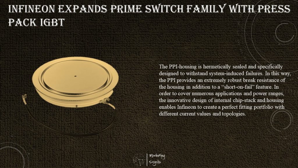
The PPI-housing is hermetically sealed and specifically designed to withstand system-induced failures. In this way, the PPI provides an extremely robust break resistance of the housing in addition to a “short-on-fail” feature. In order to cover numerous applications and power ranges, the innovative design of internal chip-stack and housing enables Infineon to create a perfect fitting portfolio with different current values and topologies.
Nexperia and KYOCERA AVX Components Salzburg Agree Partnership for GaN Automotive Power Modules
Nexperia, the expert in essential semiconductors, has announced a partnership covering gallium nitride (GaN) automotive power modules with KYOCERA AVX Components (Salzburg) GmbH, a leading international supplier of advanced electronic components for the automotive industry. This partnership agreement is the next step in the long-lasting close relationship between both companies and will focus on power components with the aim of jointly developing GaN applications for electric vehicles (EV).
As passenger vehicles become increasingly electrified, the demand for power semiconductors to provide efficient power conversion at increasingly higher power densities also grows. High voltage Power GaN FETs, when combined with innovative packaging technologies, can address the requirements for better efficiency, higher power density and reduced system cost. GaN power devices not only offer superior performance in these applications but now also provide the reliability, robustness and manufacturability expected of a mainstream technology serving a broad range of applications across multiple market segments. Nexperia manufactures GaN devices in its own facilities using mature mass production techniques which have been proven to meet the highest reliability requirements for devices to achieve AEC-Q101 certification.
Thomas Rinschede, Deputy Vice President Sensing and Control Division at KYOCERA AVX Components (Salzburg) GmbH, states: “We are very pleased to finally turn our successful and long-lasting relationship into a real partnership to strengthen KYOCERA AVX’s strategy to provide high-quality automotive compliant modules. Nexperia is a trusted and reliable partner who can deliver high-performance GaN and has shown a strong record in producing devices for the automotive market.”
Carlos Castro, Vice President and General Manager GaN Nexperia, comments: “GaN devices bring many benefits to EV applications including increased power density, improved efficiency and lower overall system cost. However, optimized packaging technology is required in order to more fully realize the benefits of GaN devices, especially in high power systems. Nexperia recognizes the advanced technology offering and leading position which KYOCERA AVX holds in the automotive industry and believes that this joint collaboration in the development of GaN automotive power modules will enable both companies to deliver superior EV power systems solutions to our customers.”
Mitsubishi Electric Adds a New Module to SiC Power Device Lineup
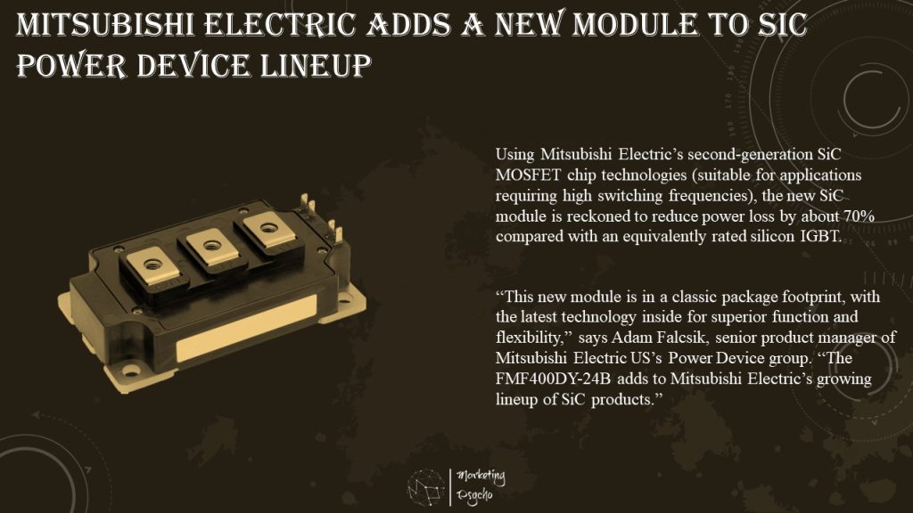
Mitsubishi Electric has launched the FMF400DY-24B, a 400A, 1200V dual silicon carbide (SiC) MOSFET power module that includes an anti-parallel, low Vf, zero-recovery-loss SiC Schottky barrier diode (SBD).
The module packages new designs into an existing industry-standard footprint (62mm x 108mm) for medical power supplies and general industrial applications. Designed for Vgs(on)=15V, the module is compatible with standard insulated-gate bipolar transistor (IGBT) gate drivers and can be seamlessly incorporated into existing mechanical layouts for easy upgrades from silicon IGBT technologies.
Using Mitsubishi Electric’s second-generation SiC MOSFET chip technologies (suitable for applications requiring high switching frequencies), the new SiC module is reckoned to reduce power loss by about 70% compared with an equivalently rated silicon IGBT.
“This new module is in a classic package footprint, with the latest technology inside for superior function and flexibility,” says Adam Falcsik, senior product manager of Mitsubishi Electric US’s Power Device group. “The FMF400DY-24B adds to Mitsubishi Electric’s growing lineup of SiC products.”
Hitachi Energy Launches Power Semiconductor Module for EVs Globally
Hitachi Energy, the global technology and market leader in power grids, announced it will launch globally RoadPak, its pioneering power semiconductor module for electric vehicles.
RoadPak sets a new benchmark in electric vehicle performance. This compact module uses state-of-the-art silicon carbide (SiC) technology to achieve exceptional levels of power density for faster charging, reliability over the vehicle’s lifetime, and the lowest possible power losses for the longest possible driving range.
“RoadPak is the result of more than 100 years of Hitachi Energy innovation and market leadership in power electronics,” said Niklas Persson, Managing Director of Hitachi Energy’s Grid Integration business. “Along with our Grid-eMotion™ Flash and Fleet EV charging systems, it builds on our commitment to take e-mobility to the next level and advance a more sustainable energy future for all.”
Tested by many EV manufacturers and with two seasons of flawless performance with the Mahindra Racing Formula E team, RoadPak is available in both the 750 volt and 1,200 volt ranges. This makes it ideal for all types of electric vehicle – regular and luxury cars, commercial vehicles, buses, agricultural EVs, heavy-duty trucks and high-performance racing cars.
“We have had the privilege of piloting this advanced power module on our Mahindra M7Electro and M8Electro racing cars over the last two years, which has proven to significantly increase performance and reliability,” said Dilbagh Gill, CEO and Team Principal of Mahindra Racing. “This high technology improvement allows us to develop next-generation state-of-the-art green automotive solutions and improve driving experience.”
Power semiconductors are a critical component in electric vehicles. They are the heart of the inverter, which converts DC power from the vehicle’s battery into the AC power that drives the motor. Reliability is key. RoadPak semiconductors are designed to operate faultlessly for more than four million start-stop cycles over the vehicle’s lifetime.
The EV market is growing exponentially. Global sales of electric cars grew 40 percent in 2020 and almost doubled in 20211. In addition, all major car manufacturers have committed to phase out their petrol and diesel vehicles by 2030 or earlier.
Hitachi Energy has two separate manufacturing sources supporting security of supply worldwide for its SiC-based power semiconductor products, including RoadPak. The company makes its own SiC chips at its semiconductor factory in Switzerland and is supported by an independent SiC chip manufacturer in the United States, thereby securing supply in terms of both volumes and geographic availability.
Hitachi Energy’s advanced semiconductor technology is a key component in its grid integration solutions that enable vast amounts of renewable energy to flow reliably through power grids and between nations. They are also key to the traction converter systems that drive high-speed electric trains and metros, and the electric vehicles that are making road transportation clean and sustainable.
Rhombus Energy Solutions to Leverage Wolfspeed’s SiC Devices for Faster EV Charging Infrastructure
Rhombus Energy Solutions, a leader in electric vehicle (EV) charging and power conversion technology, announced that Wolfspeed, Inc., the global leader in Silicon Carbide technology, will supply its EV2flexTM line of charging infrastructure products with Silicon Carbide MOSFETs, which will offer the products greater efficiency, higher power density and faster charging times.
Rhombus’ EV2flexTM infrastructure includes a family of products that enables fast, bi-directional charging and efficient energy storage. Vehicle-to-grid (V2G) charging supports power flow between the grid and the car, allowing a charged vehicle to become a power source when needed and ultimately enhancing the stability of the power grid.
“Wolfspeed has unequivocally demonstrated the high value of their Silicon Carbide MOSFETs and we are pleased to partner on advanced technology products,” said Deanne Davidson, senior vice president and general manager of Rhombus Energy Solutions. “As Rhombus continues to be the leading provider for V2G charging systems, Wolfspeed’s Silicon Carbide MOSFETs are a critical component for Rhombus to meet the demands in the growing DC fast-charging market for EVs.”
“Wolfspeed is excited to work with Rhombus, as we believe bi-directional charging is a game-changing technology for the stability of the power grid and our Silicon Carbide solutions will help accelerate that transformation,” said Jay Cameron, senior vice president and general manager of Wolfspeed Power. “Silicon Carbide increases both power system efficiency and power density to create a faster, more reliable transfer of power. Wolfspeed is leading the industry-wide transition from silicon to Silicon Carbide, which is critical as we look for more efficient and innovative ways to support the power grid, such as bi-directional EV charging.”
Wolfspeed is the preferred Silicon Carbide provider for Rhombus due to its unmatched, 30+ year history and expertise working with Silicon Carbide power devices. Wolfspeed’s 1200V Silicon Carbide MOSFETs will power Rhombus’ EV2flex-120TM charging infrastructure. Wolfspeed’s third generation MOSFETs deliver the performance and reliability required to meet a wide variety of industrial, energy and automotive applications.
Renesas to Invest and Restart Operation of Kofu Factory as 300mm Wafer Fab Dedicated for Power Semiconductors
Renesas Electronics Corporation, a premier supplier of advanced semiconductor solutions, announced that it will conduct a 90-billion-yen worth investment in its Kofu Factory, located in Kai City, Yamanashi Prefecture, Japan. While the Factory was closed in October 2014, Renesas intends to reopen the fab in 2024 as a 300-mm wafer fab capable of manufacturing power semiconductors.
As the momentum for carbon neutrality grows, demand for highly efficient power semiconductors, which supply and manage electricity, is expected to dramatically increase globally over the years. Renesas especially anticipates rapid growth in demand for electric vehicles (EVs), and therefore plans to enhance its production capacity for power semiconductors such as IGBTs, in order to contribute toward decarbonization. Once the Kofu Factory reaches its mass production, the total production capacity of Renesas’ power semiconductors will double.
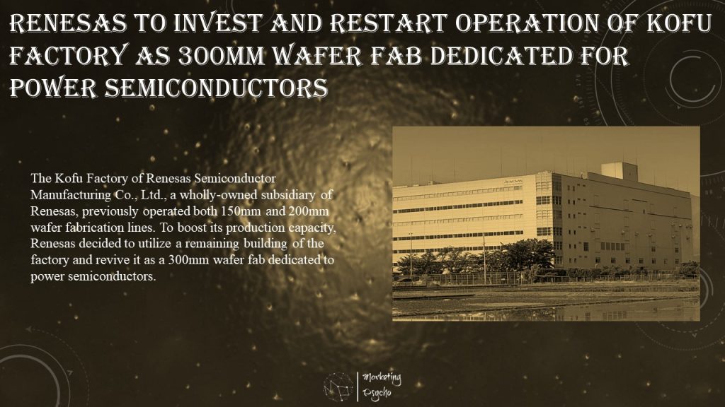
The Kofu Factory of Renesas Semiconductor Manufacturing Co., Ltd., a wholly-owned subsidiary of Renesas, previously operated both 150mm and 200mm wafer fabrication lines. To boost its production capacity, Renesas decided to utilize a remaining building of the factory and revive it as a 300mm wafer fab dedicated to power semiconductors.
“Sustainability is at our heart and with ‘To Make Our Lives Easier’ as our Purpose, we want to build a sustainable future where our semiconductor technology and solutions help make our lives easier,” said Hidetoshi Shibata, President and CEO of Renesas. “This investment enables us to have our largest wafer fabrication line dedicated to power semiconductors, which are key to realizing decarbonization. We will continue to conduct necessary investments to enhance our in-house production capability while further strengthening ties with outsource partners. To address the mid to longer term demand growth, Renesas remains committed to ensuring security of supply in order to provide our customers with the best possible support.”
With the Japanese Ministry of Economy, Trade and Industry’s Strategy for Semiconductors in consideration, Renesas plans to conduct its investment within the year of 2022, while closely coordinating with the Ministry.
Subscribe to Power Semiconductors Weekly and watch it on YouTube every Tuesday.
If you prefer a monthly update about the world of power semiconductors delivered to your e-mail address, please, subscribe to Marketing Psycho Power Semiconductors newsletter.