Power Semiconductors Weekly Vol. 60
Lucid Air – EV AC Charging ‘Powered By ROHM’
ROHM Semiconductor has announced that Lucid, an advanced luxury electric vehicle company headquartered in California, is using its silicon carbide metal-oxide-semiconductor field effect transistor (SiC MOSFET) in the ground-breaking Lucid Air. The Wunderbox, the main on-board charging unit in the Lucid Air, integrates a DC-DC converter and the Bi-directional On-Board Charger (OBC), where an advanced power factor correction circuit is capable of operating at high switching frequencies thanks to the superior performance of the SiC MOSFET. The improved performance at high frequency and high temperature of ROHM’s SCT3040K and SCT3080K SiC MOSFETs have helped Lucid to reduce the size of the design, and to reduce power losses, which results in high charging efficiency.
Lucid’s mission is to inspire the adoption of sustainable energy by creating the most captivating electric vehicles, centered around the human experience. The company’s first car, Lucid Air, is a state-of-the-art luxury sedan with a California-inspired design underpinned by race-proven technology. Customer deliveries of Lucid Air, which is produced at Lucid’s new factory in Casa Grande, Arizona, are underway. The Lucid Air was named the 2022 MotorTrend Car of the Year®. Additionally, an independent article in InsideEVs confirmed the Lucid Air’s charging capabilities. For example, when connected to DC fast chargers, they found it takes approximately 22 minutes to deliver a charge which will enable select Lucid Air models to cover 300 miles. The SiC MOSFET switched OBC can deliver up to 19.2 KW AC charging, adding up to 80 miles of range per hour.
“It was important for Lucid to form strategic alignments with key EV power device suppliers to ensure our future success. ROHM is one of the world’s leading suppliers of SiC technology, with strong technical support. We were impressed with ROHM’s strategic investments to increase the production capacity of SiC products, and its development of next generation technologies,” said Eric Bach, Senior Vice President of Product and Chief Engineer, Lucid Group. “Lucid values the close collaborative relationship with ROHM in this work.”
Added Kazuhide Ino, ROHM’s Managing Executive Officer, CSO and Director of Accounting & Finance Headquarters: “We are excited to help Lucid develop systems for electric vehicles that maximize the potential of ROHM’s SiC MOSFETs. ROHM will continue to strengthen its SiC device lineup, delivering power solutions – such as the charging systems featured in the Lucid Air – that contribute to technological innovation in next-generation automobiles. New products soon to be added, include gate driver ICs that maximize device performance.”
Alpha and Omega Semiconductor Releases 600V Super Junction MOSFETs
Alpha and Omega Semiconductor Limited (AOS), a designer, developer, and global supplier of a broad range of power semiconductors and power ICs, and digital power products, announced the release of 600V 110mOhm and 140mOhm αMOS5™ Super Junction MOSFETs in DFN8x8 Package. αMOS5 is AOS’s latest generation of high voltage MOSFET, designed to meet the high efficiency and high-density needs for Quick Charger, Adapter, PC Power, Server, Industrial Power, Telecom, and Hyperscale Datacenter applications.
Today’s Server Power design is driven by two major differentiators – high efficiency and a slim form factor to accommodate 1U, 0.5U, or even thinner systems. As higher power output is required while board space is further reduced, there are no other ways but choosing components with lower losses and small dimensions. Given the large stray inductance (larger Eon losses) and unfit height, the traditional through-hole package types are no longer the options. Typical high-power PFC and LLC stages also use gate drivers to control MOSFETs. Packages with Kelvin Sources will allow separate power and drive source connections, thus suppressing di/dt induced Vgs transients and turn-on losses. To further reduce system losses, other than minimizing magnetic and switching losses by leveraging ZVS/ZCS topologies, an increasingly adopted solution is to replace the diode bridge with high voltage MOSFETs, which serves as an Active Bridge Rectifier through the control of a driver (e.g., AOS AOZ7200).
AOS’s newly released AONV110A60 and AONV140A60 are two 600V low ohmic MOSFETs packaged in the 8mm x 8mm x 0.9mm DFN8x8 with Kelvin Source. Compared to other packages such as D2PAK, DPAK, or TO-220(F), DFN8x8 is a smaller package offering a well-balanced footprint and thermal dissipation. The 64mm² footprint makes AONV110A60 and AONV140A60 ideal for Active Bridge and high-density PFC/Flyback/LLC applications. In an internal benchmark, we compared 4 x AONV110A60 with the typical 8A GBU806 diode bridge under the 300W 90Vac scenario, the Active Bridge solution with AONV110A60 reduced the power loss by almost 50% (3.16W loss with Active Bridge vs. 6.12W loss with Diode Bridge) and increased the efficiency by 1.1%. The two DFN8x8 devices also find great fit in applications with only PFC and LLC stages, given 57% and 80% reduction in footprint and height, respectively, versus D2PAK.
Besides Server applications, AONV110A60 and AONV140A60 also target Solar Micro Inverter and Slim Adapter applications. Micro-Inverter design sees the trend of converting solar energy from two panels via one inverter, which means doubled power rating but not necessarily doubled the system size. DFN8x8 devices could help achieve this goal by paralleling and reducing effective Rdson, and accordingly, power losses. DFN8x8’s Kelvin Source would be much favored in a high Fsw inverter design, where switching losses are more significant and need to be minimized. In slim adapter designs, DFN8x8 devices, together with high Fsw controllers and planar transformers, could easily push the system density to 20W+/ in3 and efficiency up to 93%+ (with Active Bridges).
“Years ago, we could hardly imagine high voltage DFN8x8 devices widely adopted for server systems above 400W, even limited in low power SMPS, since people are used to through-hole or larger packages such as TO-220(F) or D2PAK. The power design concept has changed tremendously and rapidly with more and more DFN8x8 devices used in Active-Bridge, Tel: 408.830.9742 • Fax: 408.830.9757 • www.aosmd.com 2 PFC, Half-Bridge, and Full-Bridge topologies. DFN8x8 devices’ value proposition is clear, it is a high voltage SMD package that offers smaller form factor, better switching performance (Low Eon), higher system reliability (Low Gate Ringing), and easier board assembly.
AOS will continue to provide our customers with differentiated solutions that best serve the application needs and mission profiles from low power universal charging to high power server, solar, and telecom rectifiers,” said Richard Zhang, Director of High Voltage MOSFET Product Line at AOS.
Technical Highlights
- Low Ohmic devices packaged in 64mm² DFN8x8
- Package Thickness < 1mm
- Kelvin Source and Low Eon/Gate Oscillation
- Automated SMT assembly
- MSL Level 1
Teledyne e2v HiRel Unveils Two Space-Screened Versions of GaN HEMTs
Teledyne e2v HiRel announced the addition of new space screened versions of its popular 650 V, 60 A high reliability gallium nitride high electron mobility transistors (GaN HEMTs). The new parts go through NASA Level 1 screening flow and can be brought up to full Level 1 conformance with extra qualification testing if desired. Typical applications include battery management, DC-DC converters, and space motor drives.
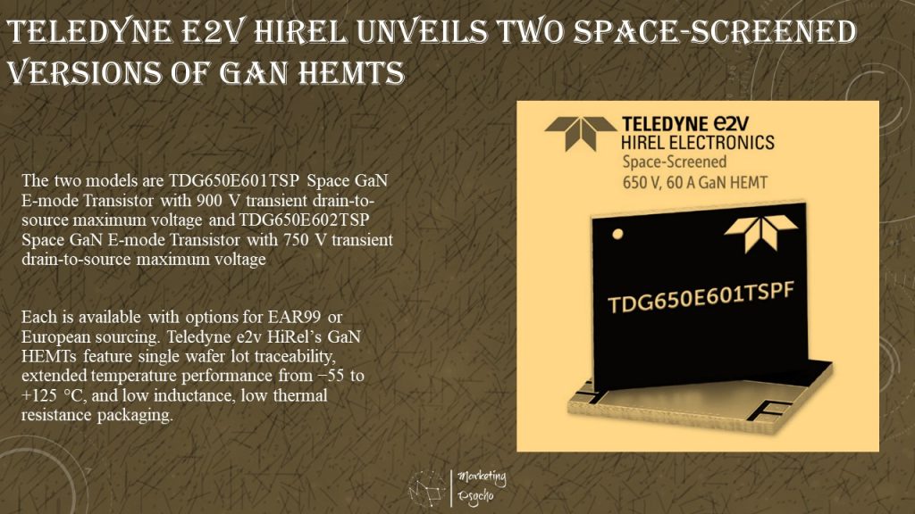
Two new parts are available, both space-grade, 650 V, enhancement mode, top-side cooled GaN-on-Silicon power transistors. The properties of GaN allow for high current, high voltage breakdown and high switching frequency, enabling high efficiency and high-power density designs.
The two models are TDG650E601TSP Space GaN E-mode Transistor with 900 V transient drain-to-source maximum voltage and TDG650E602TSP Space GaN E-mode Transistor with 750 V transient drain-to-source maximum voltage
Each is available with options for EAR99 or European sourcing. Teledyne e2v HiRel’s GaN HEMTs feature single wafer lot traceability, extended temperature performance from −55 to +125 °C, and low inductance, low thermal resistance packaging.
“Our GaN HEMT product family has been very popular with customers, and we have had many requests for catalog versions with standard space screening,” said Mont Taylor, VP of Business Development for Teledyne e2v HiRel. “Our new 650 V, 60 A parts offer 100% screening off-the-shelf, and we can do full level 1 qualification with customer SCDs”.
Gallium nitride devices have revolutionized power conversion in other industries and are now available in radiation tolerant, plastic encapsulated packaging that has undergone stringent reliability and electrical testing to help ensure mission critical success. The release of these new GaN HEMTs delivers to customers the efficiency, size, and power-density benefits required in critical aerospace and defense power applications.
Infineon’s IPOSIM Now Offers Lifetime Estimation Simulations
For many years, the Infineon Power Simulation platform (IPOSIM) has helped designers select the most suitable high-power devices based on power and thermal calculations. In IPOSIM, you can easily simulate single operating points and user-defined load profiles.
Now Infineon is extending the IPOSIM platform with the first automated Lifetime Estimation service on the market. This new premium feature enables you to digitally estimate the lifetime of Infineon power modules depending on usage and application requirements. With this lifetime estimation algorithm, you can access Infineon’s power electronics expertise online 24/7 and as often as needed during the design process.
Main Features:
Simplify your Infineon power device selection
- User-friendly flow, designed to guide you step by step in simulating with power devices
- Nineteen topologies for discs and modules available, clustered by power conversion type
- Multi-selection of up to 5 Infineon products for performance comparison
Accelerate your design iterations
- Save and share designs within your team using deep-link
- Simulation graphs with advanced scope functions for direct analysis
- Fast online simulation powered by PLECS (registered)
Soitec to Expand its Manufacturing Footprint in Bernin with SiC
Soitec (Euronext Paris), a world leader in the design and production of innovative semiconductor materials, announced a new fabrication facility at its headquarters in Bernin, France, primarily to manufacture new silicon carbide wafers which respond to key challenges of the electric vehicle and industrial markets. The extension will also support Soitec’s 300-mm Silicon-on-Insulator (SOI) activities.
The factory is to produce innovative SmartSiC™ engineered wafers developed by Soitec at the Substrate Innovation Center located at CEA-Leti in Grenoble, using Soitec’s proprietary SmartCut™ technology. The electronic chips built on this type of wafers offer compelling performance and energy efficiency gains to power supply systems. The new generation of silicon carbide wafers adds significant value for industrial applications and electric vehicles. It allows to enlarge their driving range, shorten the charging time and diminish their cost. With its SmartSiC™ products, Soitec is engaged with major silicon carbide device makers and targets to generate first revenues in the second half of calendar year 2023.
« We expect that by 2030, around 40% of all new cars will be electric. Our unique, highly performant, sustainable and cost competitive SmartSiC™ solution addresses the industrial challenges, helps to optimize energy efficiency, and will accelerate the adoption of electric vehicles, » says Paul Boudre, Soitec CEO. « This investment is a major milestone for us as SmartSiC™ is set to be another growth engine for Soitec, and a driver of the transformation of the automotive and industrial markets. »
II-VI Incorporated Accelerates Investment in Silicon Carbide Substrate and Epitaxial Wafer Manufacturing
II‐VI Incorporated, a leader in wide-bandgap semiconductors, announced that it is accelerating its investment in 150 mm and 200 mm silicon carbide (SiC) substrate and epitaxial wafer manufacturing with large-scale factory expansions in Easton, Pennsylvania, and Kista, Sweden. This is part of the Company’s previously announced $1 billion investment in SiC over the next 10 years.
The global urgency to decarbonize energy consumption is accelerating the “electrification of everything” and driving a sea change in power electronics technology with the adoption of SiC, a wide-bandgap material that enables more efficient and compact power electronics subsystems than those based on silicon. To meet the accelerating global demand for SiC power electronics, II-VI will significantly build out its nearly 300,000 square foot factory in Easton, to scale up the production of its state-of-the-art 150 mm and 200 mm SiC substrates and epitaxial wafers. Easton’s 150 mm and 200 mm SiC substrate output is expected to reach the equivalent of 1 million 150 mm substrates annually by 2027, with the proportion of 200 mm substrates growing over time. The expansion of the epitaxial wafer capacity in Kista is aimed at serving the European market.
“Our customers are accelerating their plans to intersect the anticipated tidal wave of demand for SiC power electronics in electric vehicles that we expect will come right behind the current adoption cycle in industrial, renewable energy, datacenters, and more,” said Sohail Khan, Executive Vice President, New Ventures & Wide-Bandgap Electronics Technologies. “The Easton factory will increase II-VI’s production of SiC substrates by at least a factor of six over the next five years, and it will also become II-VI’s flagship manufacturing center for 200 mm SiC epitaxial wafers, one of the largest in the world.”
II-VI will leverage its industry-leading epitaxial wafer technology developed in Kista. This technology is differentiated by its ability to achieve thick layer structures in single or multiple regrowth steps, which is ideally suited for power devices in applications above 1 kilovolt.
The Easton factory will be powered by an uninterruptible and scalable microgrid based on fuel-cell technology to provide high assurance of supply.
Infineon Webinar: Automated Lifetime Estimation of Power Semiconductors
Power modules are a core component of a power electronic system. As such, its lifetime has an important effect on the reliability of the final product. In order to understand how real mission profiles affect the power modules, complex simulations have to be performed, often pushing the tools and the methodology to their limits due to very long and highly variable profiles. For this reason, a high level of expertise in methodology and semiconductor characteristics is required. Knowing the behavior of power modules in real usage profiles has positive effects on the selection of the right power module and therefore on the reliability and optimization of the system costs.
To facilitate the design process of industrial manufacturers, Infineon has released a new digital service: IPOSIM Lifetime Estimation. Now designers can digitally estimate the lifetime of power modules whenever they need it and as many times as they need it.
In this webinar, you will gain a general understanding of the factors affecting the lifetime of power modules, and most importantly, you will get exclusive insights into the methodology and operation of IPOSIM Lifetime Estimation service.
Key Takeaways
- Understand the factors influencing the lifetime of power modules
- Get an overview of the methodology used for the lifetime calculation of power modules in the new IPOSIM Lifetime Estimation service
- Learn how to use IPOSIM Lifetime Estimation service
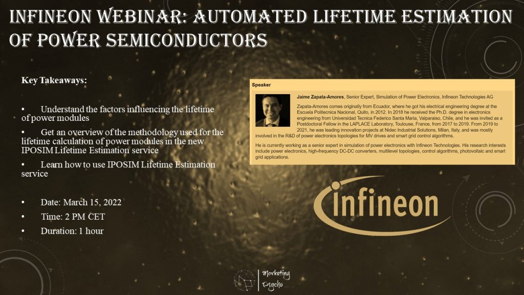
- Date: March 15, 2022
- Time: 2 PM CET
- Duration: 1 hour
Subscribe to Power Semiconductors Weekly and watch it on YouTube every Tuesday.
If you prefer a monthly update about the world of power semiconductors delivered to your e-mail address, please, subscribe to Marketing Psycho Power Semiconductors newsletter.