Power Semiconductors Weekly Vol. 55
Dual Gate Drivers Optimize and Simplify SiC and IGBT Switching Circuits
Two new dual-channel galvanically-isolated gate drivers for IGBTs and silicon-carbide (SiC) MOSFETs from STMicroelectronics save space and ease circuit design in high-voltage power-conversion and industrial applications.
The STGAP2HD for IGBTs and STGAP2SICD for SiC MOSFETs leverage ST’s latest galvanic-isolation technology to provide 6kV transient-voltage capability in a SO-36W wide-body package. In addition, ±100V/ns dv/dt transient immunity prevents spurious turn-on in electrically noisy operating conditions. The devices can deliver a powerful gate-control signal of up to 4A, with dual output pins for extra flexibility in gate driving, allowing independent adjustment of turn-on and turn-off times. The active Miller clamp prevents gate spikes during fast commutation in half-bridge topologies.
Circuit protection features include thermal protection, a watchdog for safe operation, and Under-Voltage Lockout (UVLO) per channel to prevent starting-up in a dangerous low-efficiency mode. The STGAP2SICD has a raised UVLO threshold voltage optimized for the needs of SiC MOSFETs.
Each device has an iLOCK pin for turning on both channels simultaneously in dual low-side and asymmetrical half-bridge applications. There is also interlocking to prevent shoot-through currents in conventional half-bridge circuits. Both drivers are rated for voltages up to 1200V on the high-voltage rail and have input-to-output propagation time of 75ns with high PWM accuracy.
With dedicated shutdown and brake pins, and a standby pin for power saving, ST’s new dual-channel galvanically-isolated gate drivers target applications including power supplies, drives, inverters, welders, and chargers. In addition, input pins compatible with TTL and CMOS logic down to 3.3V simplify connection to a host microcontroller or DSP.
Both the STGAP2HD and STGAP2SICD are in production now and are priced from $1.84 for orders of 1000 pieces. The EVALSTGAP2HDM and EVALSTGAP2SICD demonstration boards are also available, allowing rapid evaluation of the drivers’ features when driving a half-bridge power stage.
Power Integrations Introduces High-Voltage Switcher ICs with 1700 V SiC MOSFET
Power Integrations, the leader in high-voltage integrated circuits (ICs) for energy-efficient power conversion, announced the addition of two new AEC-Q100 qualified, 1700-volt rated ICs to its InnoSwitch™3-AQ family. The new devices are the industry’s first automotive-qualified switching power supply ICs to incorporate a silicon carbide (SiC) primary switching MOSFET. Delivering up to 70 watts of output power, the new ICs are targeted for use in 600- and 800-volt battery and fuel-cell electric passenger vehicles, as well as electric buses, trucks and a wide range of industrial power applications.
Highly integrated InnoSwitch ICs reduce the number of components required to implement a power supply by as much as 50 percent, saving significant circuit-board space, enhancing system reliability and mitigating component sourcing challenges. Devices from the award-winning InnoSwitch family are now available with a choice of cost-effective silicon, high-efficiency gallium nitride (GaN) and high-voltage SiC transistors, permitting designers to optimize their power solution across a broad range of consumer, computer, communications, industrial and automotive applications.
Peter Vaughan, director of automotive business development at Power Integrations, said: “800-volt batteries are becoming standard for EVs. Multiple vehicle systems are connected to this powerful electrical source, yet delicate electronic control circuits require just a few volts for operation and communication. InnoSwitch devices allow the electronics to safely sip from the firehose of energy available on the main bus, using minimal board area and without wasting energy. Most exciting is the opportunity to dramatically simplify the emergency power supply for the main traction inverter, which may be called upon at a moment’s notice to operate from any voltage between 30 volts and 1000 volts. Our SiC-based InnoSwitch™3-AQ devices handle this vast range with incredible ease.”
Offered in a compact InSOP™-24D package, the new ICs use a FluxLink™ feedback link, providing reinforced isolation up to 5000 VRMS for secondary-side control. FluxLink technology enables direct sensing of the output voltage, providing benefits such as accurate regulation and extremely fast transient response. The circuit will start from 30 volts without external circuitry – critical for functional safety. Additional protection features include input under-voltage, output over-voltage and over-current limiting.
The inclusion of synchronous rectification and a quasi-resonant (QR) / CCM flyback controller achieves greater than 90% efficiency, easily meeting the strictest OEM requirements. These new parts consume less than 15 mW at no-load, which is ideal for reducing self-discharge in battery management systems.
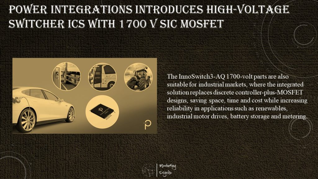
The InnoSwitch™3 1700-volt parts are also suitable for industrial markets, where the integrated solution replaces discrete controller-plus-MOSFET designs, saving space, time and cost while increasing reliability in applications such as renewables, industrial motor drives, battery storage and metering.
II-VI Qualifies 1200 V SiC MOSFET Platform to Automotive Standards and Expands Relationship with GE
II‐VI Incorporated, a leader in wide-bandgap semiconductors, announced that it has qualified its 1200 V silicon carbide MOSFET platform, on its high-quality SiC substrates, to stringent automotive standard requirements and is expanding its relationship with GE by signing a three-year technology access agreement (TAA) with GE Research to gain access to the Lab’s world-class SiC module technology and team of experts to accelerate customer design-in engagement activities.
A growing number of applications, such as in electric vehicles, renewable energy, datacenters, industrial motors, and power supplies, are driving the strong demand for SiC-based power electronics, due to their high efficiency, lower total system-level cost of ownership, higher reliability, and ability to achieve more compact system designs compared with state-of-the-art silicon-based devices. Leveraging its differentiated 150 mm SiC substrates, II-VI successfully completed the qualification of its 1200 V SiC MOSFET platform to the Automotive Electronics Council AEC-Q101 standard, exceeding it to 200°C.
“This qualification represents an important milestone that allows us to begin ramping up our commercial activities for devices in the industrial motor and renewable-energy markets, while in parallel, initiating longer-term design-in activities in the electric vehicle market,” said Sohail Khan, Executive Vice President, New Ventures & Wide-Bandgap Electronics Technologies. “The licensing of GE’s technology in 2020 allowed us to achieve our qualification milestone ahead of schedule. The technology access agreement will strengthen our relationship with GE and further accelerate our time to market as we continue to execute on our previously announced plan to grow by investing $1 billion in capacity and innovation for our SiC platform over the next ten years.”
The TAA with GE Research expands the relationship with GE by building on an earlier agreement in which II-VI licensed GE’s technology to manufacture SiC devices and modules for power electronics. The TAA will involve about a dozen of GE Research’s SiC device and systems experts and test facilities, which will be dedicated to the next phase of the commercialization of II-VI’s SiC devices and modules.
“We’re excited to enter into this new agreement, which will enable II-VI to capitalize on billions of dollars of new market opportunities for power electronics in the automotive, industrial, and other sectors,” said Vic Abate, GE’s Chief Technology Officer. “As we work with II-VI to expand its market base, we will also leverage new advancements in SiC power devices and modules to improve GE’s position with its SiC products in the aviation market and support other GE products in the energy and health care spaces that will benefit from these more capable power electronics devices.”
GE Aviation today offers a robust portfolio of SiC-based electrical power products for aerospace, industrial, and military applications. Also, GE’s other businesses, which include renewable-energy assets, grid infrastructure, and medical imaging scanners, will all see improved performance and efficiency with the integration of SiC-based power electronics platforms.
Sample dies are available now and packaged samples are scheduled to be available by mid-calendar year 2022.
STMicroelectronics to Double Investments to Meet High Chip Demand
STMicroelectronics plans to double its investments this year to up to $3.6 billion compared with $1.8 billion in 2021, buoyed by high demand that drove its earnings to beat expectations in the fourth quarter. That will include building the first production line of a new 300 mm wafer plant in Agrate, Italy.
The step up in spending stems from a global chip shortage that has hit manufacturers and fueled inflation for semiconductors, which range from low-added value chips in washing machines to sophisticated sensors in cars and smartphones.
STMicroelectronics, whose biggest clients include electric-car maker Tesla and iPhone maker Apple, expects net revenues this year in a range of $14.8 billion to $15.3 billion, a 20 percent increase at the top of the range.
STMicroelectronics’ larger peers have also fared well. Industry bellwether Texas Instruments beat market expectations and is also boosting capacity. Taiwanese chip company TSMC expects strong growth to accelerate in coming years due to booming semiconductor demand. The semiconductor bottleneck was still being felt at the start of 2022.
Toshiba to Expand Power Semiconductor Production Capacity with 300-millimeter Wafer Fabrication Facility
Toshiba Electronic Devices & Storage Corporation announced that it will construct a new 300-milimeter wafer fabrication facility for power semiconductors at its main discrete semiconductor production base, Kaga Toshiba Electronics Corporation, in Ishikawa Prefecture. Construction will take place in two phases, allowing the pace of investment to be optimized against market trends, with the production start of Phase 1 scheduled for within fiscal 2024. When Phase 1 reaches full capacity, Toshiba’s power semiconductor production capacity will be 2.5 times that of fiscal 2021.

Power devices are essential components for managing and reducing power consumption in every kind of electronic equipment, and for achieving a carbon neutral society. Current demand is expanding on vehicle electrification and the automation of industrial equipment, with very strong demand for low-voltage MOSFETs (metal oxide semiconductor field effect transistors) and IGBTs (insulated-gate bipolar transistors) and other devices. To date, Toshiba has met this demand growth by increasing production capacity on 200-milimeter lines, and expediting the start of production on 300-milimeter production lines from the first half of fiscal 2023 to the second half of fiscal 2022. Decisions on the new fab’s overall capacity and equipment investment, the start of production, production capacity and production plan will reflect market trends.
The new fab will have a quake absorbing structure; enhanced BCP systems, including dual power supply lines; and the latest energy saving manufacturing equipment to reduce environmental burdens. It will also aim to achieve the “RE100” goal of 100% reliance on renewable energy. Product quality and production efficiency will be improved by introducing artificial intelligence and automated wafer transportation systems.
Going forward, Toshiba will expand its power semiconductor business and boost competitiveness by timely investments and research and development that will allow it to respond to fast growing demand, and to contribute to a low-energy society and carbon neutrality.
Schedule (Plan)
- Construction start: Spring, 2023
- Construction complete: Spring, 2024
- Production start: within fiscal 2024
Wolfspeed Webinar: Silicon Carbide Discrete MOSFETs Push Higher Power in EV Fast Charging
Sales of electric vehicles (EV) are set to accelerate rapidly over the coming decade. With continuously improving batteries and consumers demanding quicker turnaround on charging EV’s design trends point to higher power charging blocks.
The emergence of Wide Bandgap (WBG) semiconductors like Silicon Carbide (SiC) allows better pairing of power devices for the fast-charging application. This Wolfspeed’s webinar will provide you with practical design considerations when selecting the topologies and power device with a focus on designing with discrete SiC MOSFETs beyond 25kW.
Key Takeaways:
- Design challenges of EV fast chargers
- Practical design considerations, including topology, power component selection, magnetics design, and PCB layout considerations
- Test results of Wolfspeed’s 30kW reference design
- Date: February 24, 2022
- Time: 5 PM CET
Subscribe to Power Semiconductors Weekly and watch it on YouTube every Tuesday.
If you prefer a monthly update about the world of power semiconductors delivered to your e-mail address, please, subscribe to Marketing Psycho Power Semiconductors newsletter.