Power Semiconductors Weekly Vol. 49
Update on ROHM Solution Simulator: New Thermal Analysis Function
ROHM has recently added a new thermal analysis function to ROHM Solution Simulator that allows designers of electronic circuits and systems in the automotive and industrial markets to collectively verify power devices and driver ICs thermal issues on different solution circuits.
ROHM Solution Simulator, which runs on ROHM’s website, makes it possible to carry out a variety of simulations for free – from component selection to individual device and even system-level verification. This enables easy and accurate verification of ROHM products such as SiC devices in power semiconductors, driver/power supply ICs, and passive components (i.e. shunt resistors) in solution circuits under close to actual application conditions.
ROHM released its ROHM Solution Simulator in 2020 – in line with the company’s overall focus: developing and supporting application circuits that maximize the characteristics of driver ICs and power devices designed to supply high power in the automotive and industrial equipment markets. In this context, the ROHM Solution Simulator enables full circuit verification of power semiconductor and analog ICs. The tool is free of charge, and the software has been well received for its applicability and high accuracy.
The newly added thermal analysis function can be implemented in solution circuits for devices and applications where heat is likely to become an issue in electronic circuit design. Examples are PTC heaters (heaters specifically designed for electric vehicles without internal combustion engines) equipped with IGBTs and shunt resistors as well as DC/DC converter ICs and LED drivers in order to meet the increasing demand to simulate temperature during circuit operation. This is the only simulator in the industry that enables web-based electrically and thermally coupled analysis of not only of the semiconductor chip (junction) temperature during operation, but also pin temperatures as well as thermal interference of board components on solutions circuits that include both power semiconductors and ICs along with passive components.
As a result, thermal analysis that used to take as much as a day can now be performed in about ten minutes (100x faster than conventional methods). This allows users to quickly and easily check the temperature of various parts of the device before prototyping (instead of after as is currently the case), reducing the need for rework. At the same time, the amount of development resources required for applications where heat is an issue decrease.
ROHM Solution Simulator can be used free of charge by simply registering on ROHM’s website. In addition to the simulator, the dedicated web page provides access to videos and documents required for use.
ROHM Solution Simulator Page: https://www.rohm.com/solution-simulator
Going forward, ROHM will continue to implement thermal analysis functions in solutions circuits compatible with ROHM Solution Simulator, focusing on the latest SiC devices, to further reduce the number of resources required for application development and prevent issues.
STMicroelectronics Introduces First PowerGaN Products
STMicroelectronics, a global semiconductor leader serving customers across the spectrum of electronics applications, has revealed a new family of GaN power semiconductors in the STPOWER portfolio that can significantly reduce energy use and enable slimmer designs in a huge variety of electronic products. Target applications include consumer equipment such as chargers, external power adapters for PCs, LED-lighting drivers, and power supplies inside televisions and home appliances. This equipment is produced in high volumes worldwide and, with greater efficiency, can realize significant CO2 savings. In higher-power applications, ST’s PowerGaN devices also benefit telecom power supplies, industrial motor drives, solar inverters, and electric vehicles and chargers.
“Commercializing GaN-based products is the next frontier for power semiconductors, and we are ready to realize the potential of this exciting technology. Today ST is announcing the first product in a new family, belonging to the STPOWER portfolio, that can deliver breakthrough performance for a large variety of power supplies across consumer, industrial, and automotive applications,” said Edoardo Merli, Power Transistor Macro-Division General Manager and Group Vice President of STMicroelectronics’ Automotive and Discrete Group. “We are committed to progressively building up our PowerGaN portfolio to enable customers to design more efficient, smaller power supplies everywhere.”
Gallium Nitride (GaN) is a compound wide-bandgap semiconductor material capable of supporting far higher voltages than traditional silicon without compromising on-resistance thus reducing conduction losses. Products implemented in this technology can also be switched much more efficiently, resulting in very low switching losses. The possibility of operating at higher frequencies implies the adoption of smaller passive components. All these features enable designers to cut total losses (reduce heat generated) and improve efficiency in power converters. As a result, GaN allows for miniaturization, making a PC adaptor smaller and lighter than today’s ubiquitous chargers, for example.

According to a third-party estimate, a standard mobile phone charger can be reduced by up to 40% in size when using GaN components, or it can be designed to deliver more power in the same size. Similar performance improvement in efficiency and power density can be envisioned for a broad number of applications across consumer, industrial, and automotive electronics.
The first device in ST’s new G-HEMT transistor family is the 650V SGT120R65AL with 120mΩ maximum on-resistance (RDS(on)), 15A maximum current capability, and a Kelvin source connection for optimum gate driving. It is available now in an industry-standard PowerFLAT 5×6 HV compact surface-mount package, at $3.00 (1000 pieces). Its typical applications are PC adaptors, USB wall chargers, and wireless charging.
650V GaN transistors in development are available now as engineering samples. These include the SGT120R65A2S with 120mΩ RDS(on) in an advanced laminated package, the 2SPAK™, which eliminates wire bonding to boost efficiency and reliability in high-power and high-frequency applications, as well as the SGT65R65AL and SGT65R65A2S both with 65mΩ RDS(on) in PowerFLAT 5×6 HV and 2SPAK, respectively. Volume production for these products is expected in H2 2022.
In addition, a new cascode GaN transistor, SGT250R65ALCS with 250mΩ RDS(on) in a PQFN 5×6, belonging to the G-FET family, will be available for sampling in Q3 2022.
G-FET™ transistor family is a very fast, ultra-low Qrr, robust GaN cascode or d-mode FET with standard silicon gate-drive for a wide range of power applications.
G-HEMT™ transistor family is an ultra-fast, zero Qrr e-mode HEMT, easily parallelable, well suited for very high frequency and power applications.
G-FET and G-HEMT are both belonging to the PowerGaN family of STPOWER product portfolio.
alpitronic Selects Infineon’s Easypack™ Coolsic™ Modules and Eicedriver™ X3 Drivers for Its 50 kw Hypercharger
Following the successful launch of the HYC150 and HYC300 of their hypercharger product line, alpitronic recently introduced the state-of-the-art and industry-leading 50 kW DC electric vehicle charger HYC50. It is the first wall-mounted DC charger in this power range featuring two charging ports that allow fast charging of one vehicle at 50 kW or of two vehicles simultaneously at 25 kW each. This is made possible by using EasyPACK™ CoolSiC TM MOSFET 1B and 2B modules from Infineon Technologies AG in combination with the EiceDRIVER™ X3.
“We are committed to working closely with customers like alpitronic to help them realize unique designs enabling superior system solutions,” said Dr. Peter Wawer, president of the Industrial Power Control Division at Infineon. “In addition to comprehensive system expertise and many years of experience, we offer first-class solutions such as our portfolio of EasyPACK 1B and 2B modules with the latest 1200 V CoolSiC MOSFET technology to increase the efficiency as well as the power density. The devices can be flexibly combined with suitable drivers to meet the requirements of each customer and their individual project.”
“With Infineon’s CoolSiC EasyPACK modules in combination with a perfect matching driver IC, we were able to significantly improve the efficiency of our new hypercharger,” said Philipp Senoner, co-founder and managing director of alpitronic. “We are therefore very pleased to have Infineon as a reliable and competent partner at our side, providing a wide range of CoolSiC MOSFET, gate drivers and the necessary understanding of our specific requirements.”
By using the CoolSiC technology, the HYC50 achieves up to 97 percent efficiency and enables a bidirectional design. As a result, this hypercharger is suitable for vehicle-to-grid (V2G) operation. At the same time, the charger has a compact footprint of 1250 x 520 x 220 mm³ and weighs less than 100 kg. Its compact size makes the charger ideal for indoor wall mounting, though it can also be mounted flexibly on a pedestal outdoors. The charger supports the charging standards CCS1 and CCS2 with a capacity of 150 A, CHAdeMO with a capacity of 125 A, as well as GBT.
In this particular design, Infineon’s EasyPACK 1B and 2B modules, which include CoolSiC MOSFETs, a NTC temperature sensor, and PressFIT contact pins, were able to increase power density by about 50 percent. In addition, by using CoolSiC technology, the noise level was significantly reduced from 65 dB to less than 50 dB.
Besides the necessary power devices, Infineon also provided the matching drivers. The X3 driver IC is particularly suitable for the modules in this design, offering a number of decisive advantages through its configurability and active and passive monitoring options. For instance, it enables additional sensor points for operational monitoring, with several gate drivers providing additional temperature points as well as gate voltage monitoring. Thus, the temperature and voltage can be adjusted exactly according to the requirements of the SiC MOSFETs, minimizing static conduction losses and avoiding overloads.
Furthermore, the operating points in the field can be optimized by OTA (Over-the-Air) updates – these can also influence the parameters in the gate driver. Thereby, systems in different climates can be optimized for the corresponding environmental conditions.
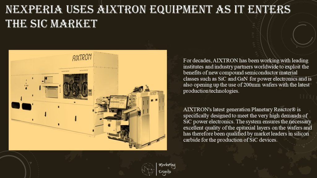
Nexperia Uses AIXTRON Equipment as It Enters the SiC Market
Nexperia, the expert in essential semiconductor, is using AIXTRON SE production technology to enter the high performance SiC device market. For volume production of silicon carbide epi wafers for SiC power devices, Nexperia requires consistently excellent epi wafer quality, even at high volumes. At the same time, costs in the production of SiC devices can be reduced due to the high throughput.
As one of the leading experts in the field of volume production of semiconductor devices, Nexperia plans to continuously expand its portfolio of silicon carbide devices. AIXTRON, one of the leading suppliers of deposition equipment to the semiconductor industry, meets the high-quality requirements of silicon carbide wafers for power electronics with its fully automated AIX G5 WW C platform.
“Wide-band-gap semiconductors such as gallium nitride and silicon carbide have unique physical properties. They enable high power density and efficiency at lower system and operating costs. SiC technology is also now advanced enough to meet the stringent requirements for mass production of devices for modern consumer and industrial products. Therefore, it is now time for Nexperia to take our next strategic step, the expansion of our portfolio to include power semiconductor devices based on silicon carbide,” says Mark Roeloffzen, General Manager of the Bipolar Discretes Group at Nexperia.
He adds: “In the future, we will also cover the value-added stage of epi-wafer production in the field of high-performance components. For this important milestone, we know that AIXTRON is the right partner for Nexperia.”
For decades, AIXTRON has been working with leading institutes and industry partners worldwide to exploit the benefits of new compound semiconductor material classes such as SiC and GaN for power electronics and is also opening up the use of 200mm wafers with the latest production technologies.
AIXTRON’s latest generation Planetary Reactor® is specifically designed to meet the very high demands of SiC power electronics. The system ensures the necessary excellent quality of the epitaxial layers on the wafers and has therefore been qualified by market leaders in silicon carbide for the production of SiC devices.
“Nexperia is positioning itself at the right time in one of the most exciting growth markets in the semiconductor industry. We are pleased that Nexperia has chosen us as a partner in this important strategic step into a new market of the future. The performance characteristics of the silicon carbide and gallium nitride material classes, with their high efficiency, offer highly attractive potential for energy savings, heat reduction, weight and system size reduction, and thus lower overall system costs,” says Dr. Felix Grawert, CEO and President of AIXTRON SE.
“SiC and GaN semiconductors offer higher energy efficiency in applications compared to conventional power electronics based on silicon and thus contribute significantly to lower CO2 emissions. The properties of the materials predestine them in particular for applications in electric vehicles and their charging stations, data centers or in the field of renewable energies such as solar and wind power plants,” adds Dr. Felix Grawert.
At the beginning of the year, Nexperia had already started a significant investment program both in the expansion of its production capacities, and in research and development worldwide. As part of its global growth strategy, planned investments in Europe this year include production efficiency improvements and the implementation of new 200mm technologies at its European wafer fabs in Hamburg, Manchester and Newport. In Hamburg, the company is investing in new technologies for the expansion of its “wide band gap” SiC power device offering.
Wuxi Leapers Semiconductor Co., Ltd. Completed 100 million yuan of A-Round Financing
On December 1, Wuxi Leapers Semiconductor Co., Ltd. officially announced: it has completed nearly 100 million yuan of A-round financing, led by Germanlink Capital, followed by Rich Land Capital and Feitu Venture Capital. This round of funds will mainly be used for R&D equipment investment in Wuxi and Japan, as well as R&D investment, management operation and market promotion.
Wuxi Leapers Semiconductor Co., Ltd., founded in 2019, focuses on the R&D, production and sales of SiC and IGBT power modules. With innovative packaging materials and technologies, Leapers provides miniaturized, lightweight and efficient power module solutions for controllers used in new energy vehicles, hydrogen vehicles, photovoltaic and other industries. At present, the company has applied for 26 patents, including 13 invention patents.
As the core device of electric energy conversion, power semiconductor is widely used in new energy vehicles, rail transit, industrial control, photovoltaic, wind power and other fields, with huge market space. China’s power semiconductor market is expected to reach $15.9 billion (about 101.5 billion yuan) this year, and the global market is expected to exceed $50 billion (about 319.3 billion yuan) by 2024, according to market research firm IHS.
Although China’s power semiconductor market occupies more than 1/3 of the global scale, but the domestic production rate of high-end power devices is very low, the reliability of high-end domestic power modules also leads to a low market share, more than 90% of the middle and high-end MOSFET and IGBT, SiC devices still rely on imports.
First, high-end power devices are mainly applied in new energy vehicles, wind power generation, photovoltaic and other fields. These fields have high requirements on the electrical design, heat dissipation, machinery, reliability, process and other aspects of the power module. The international large manufacturers such as Infineon and Mitsubishi have accumulated mature technology and competitive advantages, but the IGBT and SiC module design and manufacturing process in China are relatively backward and still in the stage of catching up.
Second, in chip design, low-power chips usually adopt single-tube current design, while high-power chips need to be integrated into the module to achieve the effect of high-power current through more chips connected in parallel. Especially in automotive applications, there is a gap between domestic and international level in related module enterprises.
It is worth mentioning that SiC semiconductor has the advantages of stable operation at high temperature, low conduction resistance, fast switching speed and good heat dissipation performance compared with traditional silicon based semiconductor. More importantly, SiC semiconductor has no mature packaging technology in the world, with broad market development prospects.
At present, Leapers’ core products cover SiC and IGBT, among which SiC for hydrogen commercial vehicles and photovoltaic, and IGBT for charging piles, industrial frequency converters, commercial vehicles and other aspects have achieved mass production. It is worth noting that, despite SiC’s advantages as a third-generation power semiconductor in terms of performance efficiency, reliability and small weight, SiC’s replacement of IGBT is mainly concentrated in the high-end application market, and in the low-end market, it is a coexistence pattern.
Leapers’ co-founder, COO Ding Xuan Ming said, the company’s third generation of power semiconductor SiC module technology level has been able to compete directly with international well-known brand products, especially its use of all-silver sintering, the use of Leapers patent chip surface connection technology of direct water-cooling structure, electrical characteristics, heat dissipation, power density has reached the international leading level.

The technological advantages of Leapers are closely related to the positive development ability of the company team. At present, the company has a research and development center in Japan, which has begun to take shape. Leapers will form a complete advanced module packaging and verification test capabilities. The company has dozens of industry experts from China and Japan covering chip design, packaging materials, packaging design, production process, module application and other fields.
Liang Xiaoguang, the founder and CEO of the company, has worked for Mitsubishi Electric, Onsemi and ZF, and has more than 16 years of R&D experience in IGBT and SiC power semiconductor, as well as a number of relevant international patents. COO Ding Xuanming, co-founder of the company, used to be director of Shanghai Electric Drive Business Division, familiar with electric vehicle customers, supply chain and quality system requirements; Co-founder Qiu Wei used to work in Richardson, has more than ten years of sales experience in the electronic device industry; Members of the Japanese R&D team have more than 20 years of semiconductor industry experience on average.
Leapers SiC products have started mass production in the second half of this year, and sales will achieve a big breakthrough next year, with over hundreds of thousands of SiC modules.
Leapers will complete mass production of SiC module products for passenger cars in 2022, in which the next generation SiC controller platform will be more than 30% smaller than modules with the same current on the market, and can also be customized according to different current requirements, covering 150KW-400kW power.
In terms of product promotion, Leapers has taken hydrogen commercial vehicles as the market breakthrough, and gradually expanded to other commercial vehicle markets, as well as photovoltaic and other industrial markets, while focusing on the layout of passenger car market.
STMicroelectronics and Politecnico di Milano Expand Semiconductor R&D Infrastructure
STMicroelectronics, a global semiconductor leader serving customers across the spectrum of electronics applications, and Politecnico di Milano (PoLiMi) inaugurated the expansion of semiconductor-manufacturing capabilities at PoliFab, the University’s micro- and nanotechnology R&D center.
Building on the long-standing collaboration between the two organizations, the PoliFab’s clean room – a facility where silicon wafers are made into semiconductor chips – has received state-of-the-art equipment from STMicroelectronics to boost joint R&D efforts in Micro Electro-Mechanical Systems (MEMS) and motion control, as well as in power electronics and galvanic isolation.
The enlarged clean-room infrastructure will make Politecnico di Milano even more attractive for talented researchers and students and contribute to fuel ST’s advances and development roadmap in semiconductor technologies including MEMS, where the Company is a world leader with over 15 billion devices sold to date. With the core of ST’s global MEMS R&D operations located in Lombardy, close to Milan, the cooperation with PoliFab aims at setting up a center of excellence for studies and research on advanced materials for MEMS in the region.
The ongoing collaboration also encompasses investments in staff and programs, with ST supporting scholarships and the recruitment of professors and researchers, as well as financing joint research projects.
With the new spaces inaugurated, the total classified area of PoliFab spans 610 sq meters, plus annexed characterization laboratories, thus making it comparable to analogous facilities of the best European research institutions.
“We are pioneering a new model for “fast technology transfer” based on the realization of a joint research and innovation infrastructure where top-class semiconductor equipment, the very same used in a semiconductor fab, is made available to researchers and students,” said Riccardo Bertacco, director of Polifab. “Polifab 2.0 is a physical site where exciting scientific ideas can meet state-of-the-art semiconductor technology, thus speeding-up both fundamental research and its technology transfer.”
“Today’s event marks a significant milestone in building an Italy-unique, world-class semiconductor innovation hub that can contribute to ST’s R&D efforts in multiple areas including MEMS and sensors, one of the most promising technologies that enable digital transformation and the Internet of Things,” said Anton Hofmeister, Group Vice President and General Manager, R&D and Strategy for the Analog and MEMS Sub-Groups, STMicroelectronics. “The successful collaboration with Politecnico is part of our global innovation strategy to foster high-caliber talent and facilitate industry-academia joint research programs as key elements of success in the global semiconductor market.”
AspenCore Releases Guide to Silicon Carbide: Enabling a Smart Energy Future
Silicon Carbide (SiC), a wide-bandgap semiconductor, is driving a profound transformation of power electronics and clean energy systems. Its superior physical and electrical properties are already making a mark in electric vehicles, renewable energy, motor control, and aerospace/defense applications.
This 145-page guide offers a detailed analysis of the market trends and an in-depth discussion of key aspects of SiC power technology.
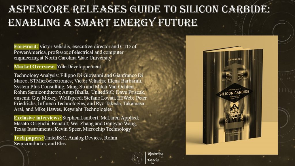
Foreword: Victor Veliadis, executive director and CTO of PowerAmerica, professor of electrical and computer engineering at North Carolina State University
Market Overview: Yole Développement
Technology Analysis: Filippo Di Giovanni and Gianfranco Di Marco, STMicroelectronics; Victor Veliadis; Elena Barbarini, System Plus Consulting; Ming Su and Mitch Van Ochten, Rohm Semiconductor; Anup Bhalla, UnitedSiC; Dave Priscak, onsemi; Guy Moxey, Wolfspeed; Stefano Lovati, EEWeb; Peter Friedrichs, Infineon Technologies; and Ryo Takeda, Takamasa Arai, and Mike Hawes, Keysight Technologies
Exclusive interviews: Stephen Lambert, McLaren Applied; Masato Origuchi, Renault; Wei Zhang and Gangyao Wang, Texas Instruments; Kevin Speer, Microchip Technology
Tech papers: UnitedSiC, Analog Devices, Rohm Semiconductor, and Eles
Subscribe to Power Semiconductors Weekly and watch it on YouTube every Tuesday.
If you prefer a monthly update about the world of power semiconductors delivered to your e-mail address, please, subscribe to Marketing Psycho Power Semiconductors newsletter.