Power Semiconductors Weekly Vol. 39
New Infineon EasyPACK™ 2B EDT2 Power Module
Infineon Technologies AG introduced the automotive qualified EasyPACK™ 2B EDT2, a flexible and scalable half-bridge power module. Depending on inverter conditions, this 750 V device can reach a maximum power of up to 50 kW and 230 A rms. With its featured specs, the module is optimized for inverter applications in hybrid and electric vehicles.
Over the past ten years, Infineon has sold more than 50 million EasyPACK modules with various chipsets for a wide range of industrial and automotive applications. With the introduction of the EDT2 (Electric Drive Train) technology in this package and full automotive qualification, Infineon is now expanding the application range of the module family to include traction inverters. The key feature of the EDT2 technology is the higher efficiency at low-load conditions. An EDT2 chip ensures significantly lower losses than current products on the market and even outperforms Infineon’s previous chip generation by 20 percent.
Another unique feature of the EasyPACK is the plug-and-play approach, which simplifies module integration. In addition, compared to classic through-hole discrete packages as well as the HybridPACK™ 1, soldering of the pins is no longer required. Infineon’s PressFIT contact technology enables a reduction in mounting time. Thanks to the package size, three EasyPACK 2Bs require 30 percent less surface area than a HybridPACK 1. For this reason, they offer not only a very compact but also a cost-effective design. Furthermore, the EasyPACK 2B EDT2 is fully qualified to the AQG324 standard.
The new EasyPACK 2B EDT2 module FF300R08W2P2_B11A will be available starting in October 2021.
New Way of Detecting Transistor Defects
Researchers at the National Institute of Standards and Technology (NIST) and collaborators have devised and tested a new, highly sensitive method of detecting and counting defects in transistors — a matter of urgent concern to the semiconductor industry as it develops new materials for next-generation devices. These defects limit transistor and circuit performance and can affect product reliability.
A typical transistor is, for most uses, basically a switch. When it’s on, current flows from one side of a semiconductor to the other; switching it off stops the current. Those actions respectively create the binary 1s and 0s of digital information.
Transistor performance critically depends on how reliably a designated amount of current will flow. Defects in the transistor material, such as unwanted “impurity” regions or broken chemical bonds, interrupt and destabilize the flow. These defects can manifest themselves immediately or over a period of time while the device is operating.
Over many years, scientists have found numerous ways to classify and minimize those effects.
But defects become harder to identify as transistor dimensions become almost unimaginably small and switching speeds very high. For some promising semiconductor materials in development — such as silicon carbide (SiC) instead of silicon (Si) alone for novel high-energy, high-temperature devices — there has been no simple and straightforward way to characterize defects in detail.
“The method we developed works with both traditional Si and SiC, allowing us for the first time to identify not only the type of defect but the number of them in a given space with a simple DC measurement,” said NIST’s James Ashton, who conducted the research with colleagues at NIST and Pennsylvania State University. They published their results on October 6th in the Journal of Applied Physics. The research focuses on interactions between the two kinds of electrical charge carriers in a transistor: negatively charged electrons and positively charged “holes,” which are spaces where an electron is missing from the local atomic structure.
When a transistor is functioning correctly, a specific electron current flows along the desired path. (Holes can also form a current. This research explored electron current, the most common arrangement.) If the current encounters a defect, electrons are trapped or displaced, and can then combine with holes to form an electrically neutral area in a process known as recombination.
Each recombination removes an electron from the current. Multiple defects cause current losses that lead to malfunction. The goal is to determine where the defects are, their specific effects, and — ideally — the number of them.
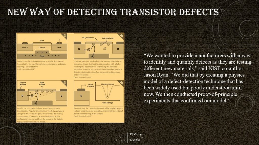
“We wanted to provide manufacturers with a way to identify and quantify defects as they are testing different new materials,” said NIST co-author Jason Ryan. “We did that by creating a physics model of a defect-detection technique that has been widely used but poorly understood until now. We then conducted proof-of-principle experiments that confirmed our model.”
In a classic metal oxide semiconductor design (see figure), a metal electrode called the gate is placed atop a thin insulating silicon dioxide layer. Below that interface is the bulk body of the semiconductor.
On one side of the gate is an input terminal, called the source; on the other is an output (drain). Scientists investigate the dynamics of current flow by changing the “bias” voltages applied to the gate, source and drain, all of which affect how current moves.
In the new work, the NIST and Penn State researchers concentrated on one particular region that is typically only about 1 billionth of a meter thick and a millionth of a meter long: the boundary, or channel, between the thin oxide layer and the bulk semiconductor body.
“This layer is hugely important because the effect of a voltage on the metal overtop of the oxide of the transistor acts to change how many electrons are within the channel region under the oxide; this region controls the resistance of the device from source to drain,” Ashton said. “The performance of this layer is dependent on how many defects exist. The detection method we investigated was previously unable to determine how many defects were within this layer.”
One sensitive method to detect defects in the channel is called electrically detected magnetic resonance (EDMR), which is similar in principle to medical MRI. Particles such as protons and electrons have a quantum property called spin, which makes them act like tiny bar magnets with two opposite magnetic poles. In EDMR, the transistor is irradiated with microwaves at a frequency about four times higher than a microwave oven. Experimenters apply a magnetic field to the device and gradually vary its strength while measuring the output current.
At exactly the right combination of frequency and field strength, electrons at defects “flip” — reverse their poles. This causes some to lose enough energy that they recombine with holes at defects in the channel, reducing the current. The channel activity can be hard to measure, however, because the high volume of “noise” from recombination in the bulk of the semiconductor.
To focus exclusively on activity in the channel, researchers use a technique called bipolar amplification effect (BAE), which is achieved by arranging the bias voltages applied to the source, gate and drain in a particular configuration (see figure). “So, because of the biasing we use in BAE and because we measure current levels at the drain,” Ashton said, “we can eliminate interference from other things going on in the transistor. We can select just defects that we care about within the channel.”
The exact mechanism by which BAE operates was not known until the team developed its model. “The only measurement results were qualitative — that is, they could tell the kinds of defects in the channel but not the number,” said co-author Patrick Lenahan, a distinguished professor of engineering science and mechanics at Penn State.
Before the model of BAE, the scheme was used strictly as a resource for applying voltages and controlling currents for EDMR measurements, which is useful for a more qualitative defect identification. The new model enables BAE as a tool to quantitatively measure the number of defects and to do so with just currents and voltages. The parameter of importance is the interface defect density, which is a number that describes how many defects are within some area of the semiconductor-oxide interface. The BAE model gives researchers a mathematical description of how the BAE current is related to the defect density.
The model, which the researchers tested in a set of proof-of-concept experiments on metal oxide semiconductor transistors, makes quantitative measurements possible. “Now we can account for the variation in charge carrier distribution throughout the channel region,” Ashton said. “This opens up the possibilities of what can be measured with a simple electrical measurement.”
“This technique can provide unique insight into the presence of these destabilizing transistor defects and a path to mechanistic understanding of their formation,” said Markus Kuhn, formerly at Intel and now senior director of semiconductor metrology and fellow at Rigaku, who was not involved in the research. “With such knowledge, there would be greater opportunity to control and reduce them in order to improve transistor performance and reliability. This would be an opportunity to further enhance design of the chip circuitry and device performance leading to better performing products.”
$18M NSF Grant to Build National Semiconductor Fabrication Facility
Engineering researchers led by Distinguished Professor Alan Mantooth have received $17.87 million from the National Science Foundation to build and operate a national silicon carbide research and fabrication facility at the University of Arkansas.
“The national impact of having a fabrication facility such as this is enormous,” Mantooth said. “The country that leads the world in advancing silicon carbide semiconductor design and fabrication will also lead the race to market nearly all new game-changing technologies, including those used by the military, as well as general electronic devices that are essential to our economy.”
The unique and open-access facility at the U of A will fill a void in U.S. production of integrated circuits made with silicon carbide, a powerful semiconductor well suited for higher temperature environments. Silicon carbide has been studied for a long time, but until recently efforts to use it as a fully developed semiconductor have been stunted by the unavailability of high-quality silicon carbide wafers. Currently, all silicon carbide fabrication facilities in the U.S. are for internal use only, and U.S. research and development of silicon carbide integrated circuits relies on international fabrication.
The U of A facility will provide domestic opportunities for prototyping, proof-of-principle demonstrations and device design. It will be the only openly accessible fabrication facility of its kind in the U.S., meaning its facilities and services will be available to external researchers.
The NSF funding will pay for infrastructure, equipment, technology installation and enhancements to current facilities to accommodate new equipment. The funding will also cover three full-time staff members, a post-doctoral researcher for four years and miscellaneous funds for set up and operating equipment.
Mantooth and other U of A electrical engineering researchers have decades of experience working with silicon carbide. They are one of only a few university research groups capable of developing integrated circuits with the powerful semiconductor. Combining this expertise with cutting-edge equipment and infrastructure will enable the production of superior integrated circuits for lighter and faster electronic systems, which will also be more energy efficient and heat resistant.
For many years, integrated circuits for most electronics devices have been made with silicon only. Silicon carbide is transforming the power electronics industry with its superior physical properties — an exceptionally strong physical bond providing high mechanical, chemical and thermal stability. Its wide band gap — the movement of electrons and photons within energy bands — and high thermal stability also allow silicon carbide-based devices to function at extreme temperatures.
The facility will provide integrated circuits, sensors and devices for military and industrial applications such as solar inverters, electronics for cars – both electric and gas-powered – and systems used in heavy transportation and construction equipment, such as bulldozers. Electronics developed at the facility will also enable systems used in geothermal and space exploration.
The facility will train the next generation of semiconductor researchers and engineers who can work in both the silicon and silicon carbide semiconductor industries. Students at all degree levels will be given research opportunities and be exposed to a high-need area of science and technology. The research will also engage underrepresented students in this new and burgeoning area of electronics.
Co-principal-investigators on this project are Greg Salamo, Distinguished Professor of physics, Zhong Chen, associate professor of electrical engineering, Shannon Davis, business and operations manager in the Department of Electrical Engineering, and John Ransom, director of silicon carbide technology at X-FAB in Lubbock, Texas.
General Motors and Wolfspeed Forge Strategic Supplier Agreement
General Motors and Wolfspeed announced a strategic supplier agreement to develop and provide silicon carbide power device solutions for GM’s future electric vehicle programs. Wolfspeed’s silicon carbide devices will enable GM to install more efficient EV propulsion systems that will extend the range of its rapidly expanding EV portfolio.
The silicon carbide will specifically be used in the integrated power electronics contained within GM’s Ultium Drive units in its next-generation EVs.
As a part of the agreement, GM will participate in the Wolfspeed Assurance of Supply ProgramTM (WS AoSP), which is intended to secure domestic, sustainable and scalable materials for EV production.
“Our agreement with Wolfspeed represents another step forward in our transition to an all-electric future,” said Shilpan Amin, GM vice president, Global Purchasing and Supply Chain. “Customers of EVs are looking for greater range, and we see silicon carbide as an essential material in the design of our power electronics to meet customer demand. Working with Wolfspeed will help ensure we can deliver on our vision of an all-electric future.”
“Our agreement with GM further demonstrates the automotive industry’s commitment to delivering innovative EV solutions to the market and using the latest advances in power management to improve overall vehicle performance,” said Gregg Lowe, CEO of Wolfspeed. “This agreement ensures long-term supply of silicon carbide to GM to help them deliver on their promise of an all-electric future.”
The silicon carbide power device solutions will be produced at Wolfspeed’s 200mm-capable Mohawk Valley Fab in Marcy, New York, which is the world’s largest silicon carbide fabrication facility. Launching in early 2022, this state-of-the-art facility will dramatically expand capacity for the company’s silicon carbide technologies, which are in increasing demand for EV production and other advanced technology sectors around the world.
The widespread adoption of silicon carbide as an industry standard semiconductor for transportation supports the automotive industry’s rapid transition to clean energy vehicles. Silicon carbide enables greater system efficiencies that result in longer EV range while lowering weight and conserving space. Wolfspeed’s technology is fueling electric propulsion systems across the entire voltage spectrum – from 400V to 800V – and beyond.
Navitas Shenzhen Expands 300% to Support Extraordinary China Revenue Growth and Accelerate High-Power GaN Applications
Navitas Semiconductor, the industry-leader in gallium nitride (GaN) power integrated circuits (ICs), has announced the opening of a new office in Shenzhen, China which offers a 300% increase in capabilities to support extraordinary revenue growth in that region. The state-of-the-art facility offers significant engineering capacity for Navitas Semiconductor to co-develop GaN-based power systems with customers and design partners. This investment supports the rapid growth of GaN mobile fast chargers, as well as the company’s recently-announced expansion plans to enable GaN-based data centers, solar installations and electric vehicles, which represent a multi-$B market opportunity for the company.

Gallium nitride (GaN) is a next-generation semiconductor technology that runs up to 20x faster than legacy silicon, and enables up to 3x more power and 3x faster charging in half the size and weight. Navitas Semiconductor GaNFast™ power ICs integrate GaN power and drive plus protection and control to deliver simple, small, fast and efficient performance. With over 130 patents issued or pending, and significant trade secrets including a proprietary process design kit (PDK), Navitas believes it has a multi-year lead in next-generation GaN power ICs.
Data center upgrades from legacy silicon to GaN are estimated to save almost $2B/year in electricity costs, while GaN adoption in solar microinverters has been estimated by Enphase Energy to enable 10x faster switching and a significant reduction in costs. Per-vehicle GaN content in passenger EVs is estimated as $50 for on-board fast chargers, $15 for DC-DC converters and then up to $200 for later adoption in traction drive.
“Alongside Hangzhou and Shanghai, the new state-of-the-art Shenzhen office is another, significant addition to Navitas China,” said Charles (Jingjie) ZHA, VP and general manager of Navitas China. “Chinese demand for next-generation power systems is growing exponentially and with the world’s only fully-integrated GaN power ICs, Navitas is in a fantastic position to capitalize on that growth. The new facilities demonstrate our commitment to support expanded customer demands in China.”
Navitas Semiconductor new office is in the iconic Baidu International Building, in the high-density Nanshan District. The design itself is an interpretation of ancient Chinese poetry into the binary codes that power the digital age, while also representing the client’s corporate temperament to the world. The building won the Council on Tall Buildings and Urban Habitat 2019 award for sustainable and healthy cities, which reflects Navitas Semiconductor goal to “Electrifying our World™”. Navitas estimates that each GaN power IC shipped saves 4kg of CO2 emissions vs. legacy silicon chips.
Subscribe to Power Semiconductors Weekly and watch it on YouTube every Tuesday.
If you prefer a monthly update about the world of power semiconductors delivered to your e-mail address, please, subscribe to Marketing Psycho Power Semiconductors newsletter.