Power Semiconductors Weekly Vol. 38
Toshiba’s New Simulation Technology Shortens Verification Times for Automotive Semiconductors by about 90%
Toshiba Electronic Devices & Storage Corporation (“Toshiba”) has developed a model-based development (MBD) simulation technology that shortens verification times for automotive semiconductors by about 90 percent. The technology allows automotive equipment developers to quickly evaluate designs using Toshiba’s automotive semiconductors, helping to shorten development times.
As electric vehicles grow in popularity and advanced driver-assistance systems become standard, automotive equipment is growing increasingly advanced and complicated. Model-based development, a development methodology that uses software to simulate models and evaluate performance in real-time, is helping product developers to refine complex design processes. In the automobile industry, MBD contributes to development advances by simultaneously progressing design and verification prior to making prototypes.
MBD separates functions into blocks and verifies total vehicle behavior by connecting each block. Detailed simulation models that include the behavior of semiconductors in individual blocks are required to verify heat and electromagnetic interference (EMI), essential parameters for assessing the performance of automotive equipment. However, as models become more detailed and precise, verification times are growing longer.
Toshiba took a long hard look at its current evaluation and verification technology for automotive equipment. Sub-systems like electric power steering comprise semiconductor-based electronic circuits that work in microseconds along with mechanical components, gears and shafts, that work in milliseconds. Toshiba’s current technology simulates the electronic circuits and mechanical components at the same time, on a microsecond basis, results in a large number of unnecessary and time-consuming calculations in the mechanical components. The technology is also complicated because it adopts the SPICE model—Simulation Program with Integrated Circuit Emphasis—that defines over 100 parameters for the simulation of semiconductor behavior.
Toshiba’s new modeling technology, “Accu-ROM™”, separately calculates the electronic circuits and the mechanical components. First it verifies the mechanical components, then simplifies the model for mechanical components and finally verifies the total system, including its electric circuits. This approach eliminates unnecessary calculations.
In evaluating the electric circuits, the model automatically generates a Very High speed integrated circuit Hardware Description Language-Analog Mixed Signal (VHDL-AMS) model from the SPICE model. VHDL-AMS model allows the verification range to be limited to essential parameters, such as heat and EMI noise, shortening the verification time. For example, verification of a power steering system with Toshiba’s current technology takes 32 hours 51 minutes, but that falls to 3 hours 27 minutes with the new technology.
Toshiba will use the new technology to promote development of high-heat dissipation and low noise automotive semiconductors, and to provide its customers with a development environment which makes it easier to use Toshiba’s products. In addition to automotive applications, Toshiba will use the new technology in semiconductors for other applications, such as industrial equipment and home appliances.
High-Voltage GaN-on-Silicon HEMT Reaches 300mm
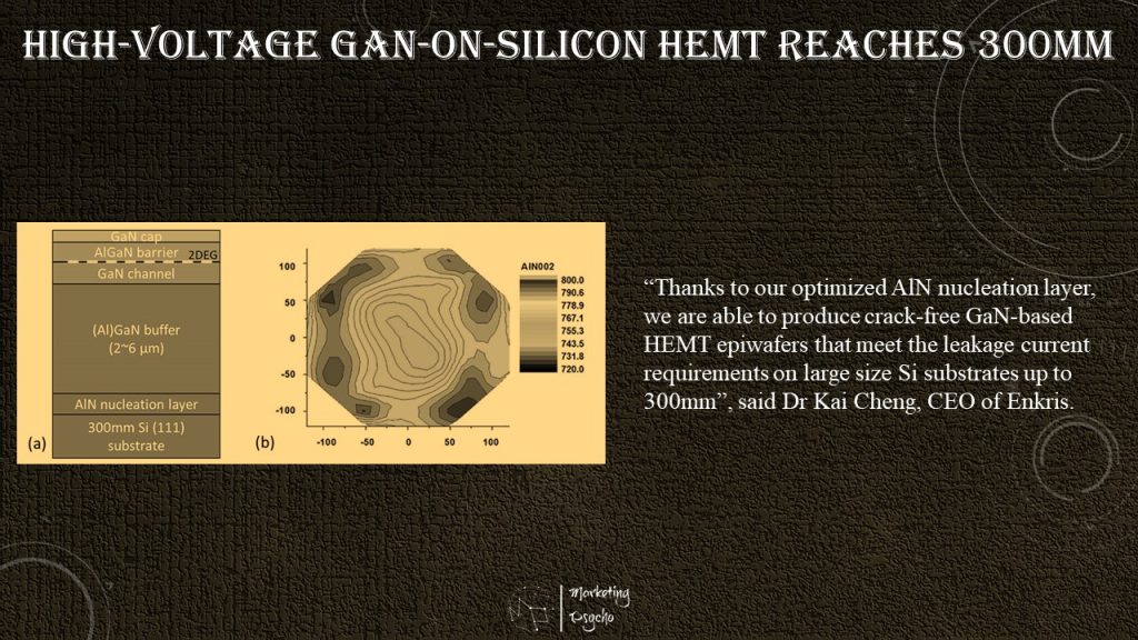
A GaN wafer epi-foundry with headquarters located at Suzhou Industrial Park, China, Enkris Semiconductor announced that it has demonstrated a series of high quality 300mm GaN-on-Si HEMT epiwafers of excellent thickness uniformity and low wafer bow for 200V, 650V and 1200V power applications, paving the way for device processing using more sophisticated 300mm CMOS-compatible lines.
The advances in the GaN epitaxy on large size Si substrates have enabled GaN-on-Si power devices with impressive performance and reliability by combing the full advantage of both the remarkable properties of GaN and of production in a CMOS compatible processing line. Nowadays, commercial GaN power devices based on GaN-on-Si HEMT technology platform have gained a tremendous momentum to enter a wide range of applications such as consumer electronics, Industrial electronics, Data Centre, Energy, Automotive & Mobility etc. Driven by cost reduction and more sophisticated integrated circuits design, the industry is moving towards larger wafer size.
Following its successful launch of commercial 200mm GaN-on-Si HV HEMT epiwafers in 2014, Enkris Semiconductor have successfully transferred its AlGaN/GaN HEMT epitaxy process to 300mm Si substrates, while maintaining the excellent thickness uniformity and low wafer bow within 50µm. The vertical voltage breakdown measurements suggest the wafers are suitable for 200V, 650V and 1200V power applications.
“Thanks to our optimized AlN nucleation layer, we are able to produce crack-free GaN-based HEMT epiwafers that meet the leakage current requirements on large size Si substrates up to 300mm”, said Dr Kai Cheng, CEO of Enkris. “Despite the challenges in epitaxy process, strain management and defect control when moving to 300mm wafer size, we have achieved excellent structural quality and electrical properties in the AlGaN/GaN HEMT structures. This will certainly encourage the development of high-power integrated circuits to yield system-on-chip and further reduce the cost of GaN power devices.”
Showa Denko Concludes Long-Term Contract to Supply SiC Epitaxial Wafers for Toshiba
Showa Denko K.K. (SDK) has concluded a long-term supply contract with Toshiba Electronic Devices & Storage Corporation (Toshiba), a Japanese electronic device manufacturer providing highly efficient SiC-power-semiconductor based power devices for the global market, to supply SiC epitaxial wafers for power semiconductors (SiC epi-wafers) for two and a half years with an optional extension clause.
Toshiba has been developing and commercializing various kinds of SiC-based power devices including inverters for railcars, while adopting SiC epi-wafers manufactured by SDK as main material for SiC-based Schottky barrier diode (SiC SBD) and SiC-based metal-oxide-semiconductor field-effect transistor (SiC MOSFET).
Toshiba decided to conclude this long-term contract because the company appreciated homogeneity in properties and low density of surface defects of SiC epi-wafers manufactured by SDK. This long-term contract will further strengthen technical cooperation between SDK and Toshiba on improvement in performance of SiC epi-wafers. In addition, SDK expects that Toshiba’s adoption of SiC epi-wafers manufactured by SDK will help SDK to expand its SiC epi-wafer business further.
As the largest independent manufacturer of SiC epi-wafers (estimated by SDK), and under a motto of “Best in Class,” the Showa Denko Group will continue coping with rapid expansion of the market for SiC epi-wafers and providing the market with high-performance and highly-reliable products, thereby contributing to the propagation of SiC power semiconductors which save energy with small power loss and less heat generation.
SUMCO Announced Issuance of New Shares to Support Production of Silicon Wafers
SUMCO Corporation announced that it has resolved, at the meeting of the board of directors held on September 30, 2021, to issue new shares of the Company through a public offering.
The Company and its group companies produces high quality silicon wafers used in semiconductor devices, and has a wide range of product development capabilities and technological capabilities, covering large to small diameter silicon wafers, and by establishing a stable supply system through making the best use of such capabilities, the Company Group contributes to the development of society.
In particular, SUMCO is concentrating on the enhancement and improvement of its technological capabilities to meet the extremely strict quality and cost demands of customers, and is striving to raise the Company’s standing in the semiconductor silicon wafer industry. Against the backdrop of continued strong demand for semiconductors used for 5G, smartphones, data centers, automobiles and so on, demand for 300 mm silicon wafers is expected to continue to grow steadily.
The supply that SUMCO can provide with the Company Group’s current manufacturing facilities is not able to keep up with demand, and the market for 300 mm leading-edge silicon wafers, which are compatible with the most advanced technologies that are the driving force for improving the performance of semiconductors, is especially expected to achieve higher levels of growth.
Based on these circumstances, SUMCO will continue to appropriately implement its policy of raising the production capacity gradually (the “Successive Capacity Expansions”) in response to customer demand to fulfill supply responsibilities to them, while taking into consideration forecasts for supply and demand for the 300 mm leading-edge silicon wafer market from time to time and the length of time, etc. required for the construction and expansion of manufacturing facilities.
II-VI Incorporated Wins Excellent Partner Awards from Sumitomo
II‐VI Incorporated, a global supplier of silicon carbide substrates and devices, announced that it received two Excellent Partner Awards, from Sumitomo Electric Industries, Ltd. (SEI), and its subsidiary, Sumitomo Electric Device Innovations, Inc. (SEDI), for their fiscal year 2020.
SEI and SEDI each announced their award, respectively, on September 8 and 15, 2021, in recognition of II-VI’s responsiveness and scalability, which contributed significantly to the expansion of Sumitomo’s business.
“II-VI is proud to receive these two awards from Sumitomo and would like to thank our teams for their dedication to excellence that made it possible,” said Dr. Chuck Mattera, Chief Executive Officer, II-VI Incorporated. “The awards reflect our strong partnership with Sumitomo and our ability to expand production capacity in response to their needs.”
“We are pleased to express our gratitude to II-VI for its notable contributions,” said Osamu Inoue, President and COO of Sumitomo Electric Industries, Ltd. “We will continue to strengthen the partnership between our valued suppliers and the Sumitomo Electric Industries Group and strive to further mutually expand our business.”
II-VI and Sumitomo are also collaborating to establish a vertically integrated, 150 mm wafer fabrication platform to manufacture state-of-the-art gallium nitride (GaN) on SiC high-electron-mobility transistor (HEMT) devices that will enable next-generation wireless networks. II-VI’s leadership in 150 mm compound semiconductor manufacturing, combined with SEDI’s leadership in GaN RF device technology, will allow II-VI and SEDI to drive best-in-class performance, greater scale, and competitive costs for 5G RF solutions.
Keysight Technologies, National Central University Optical Sciences Center, Establish Third-generation Semiconductor R&D and Test Open Laboratory
Keysight Technologies, Inc., a leading technology company that delivers advanced design and validation solutions to help accelerate innovation to connect and secure the world, and National Central University Optical Sciences Center (NCUOSC) announced a collaboration to improve the design and test validation efficiency of gallium nitride (GaN) and silicon carbide (SiC) applications, accelerating the pace of 5G and electric vehicle (EV) innovation.
Wide band gap (WBG) materials, such as GaN and SiC, offer rapid switching speeds, low loss and withstand high temperature and voltage characteristics. As a result, these materials are leveraged in consumer power products, fast charging, electric vehicles and rail transit, as well as 5G infrastructures and data center servers. However, these advantages increase the complexity of design and testing.
NCUOSC successfully used Keysight’s PD1500A Dynamic Power Device Analyzer/Double Pulse Tester (DPT) platform to establish a third generation WBG semiconductor open laboratory to improve developing and testing efficiency. As the JEDEC, a global leader in developing open standards and publications for the microelectronics industry, continues to define the dynamic testing of WBG devices, standardized tests are starting to emerge. The Keysight PD1500A DPT determines the key performance parameters, which match all standards, such as turn-on/off and switching characteristics, dynamic on-resistance, dynamic current and voltage, as well as reverse recovery, gate charge and device output characteristics.
“Keysight is happy to work with NCUOSC to help engineering teams characterize, understand, integrate, deploy and drive innovations for next-generation semiconductor technologies,” said Thomas Goetzl, vice president and general manager of Keysight’s Automotive and Energy Solutions business unit.
Reliable and repeatable measurements are critical to accelerating design and validation for new technologies, including wide-bandgap semiconductors. Keysight’s PD1500A DPT intelligent functions, such as fully automatic parameter extraction software based on IEC and JEDEC standards, loop testing, voltage and current sweep testing, and automatic high temperature testing can help drive future innovations.
“Keysight’s PD1500A DPT enables NCUOSC to reliably characterize wide-bandgap devices and effectively innovate GaN and SiC applications. Its safety protection, scalable and optional test fixtures deliver the flexibility we needed for future expansions,” said Professor Yue-Ming Hsin, Director of NCUOSC. “In addition to the PD1500A, we also setup the Keysight B1505A/N1265A Power Device Analyzer/Curve Tracer to serve the complete and crucial characterizations of WBG semiconductors. It’s our pleasure to collaborate with Keysight and contribute to the ecosystem of 5G/6G and electric vehicles.”
Automotive Semiconductor Trends 2021
Driven by numerous factors, the car industry is undergoing dramatic changes.
A chip shortage resulting from a conjunction of many events started in November 2020 and could last beyond H2 2022. A direct consequence is a chip price increase of up to 20% and disruption in the supply chain.
In 2021, many countries announced aggressive plans to reduce CO2 emissions through car electrification. Therefore, in the next 15 years, OEMs will have to shift most of their production from ICE (Internal Combustion Engine) cars to EV/HEVs worldwide. This evolution, along with more semiconductor content driven by C.A.S.E. (Connectivity, ADAS, Sharing, Electrification), will favor the coming of new entrants.
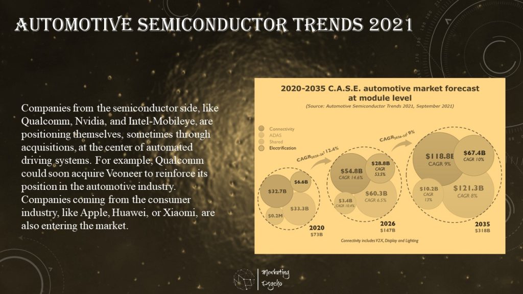
The value of semiconductors (at the chip level) in cars will grow from $34.4B in 2020 to $78.5B in 2026, a 14.75% CAGR. The largest growth will be in EVs due to the major shift to electrification.
The development of electric vehicles and self-driving technologies naturally attracts OEMs and Tier-1 component suppliers. Therefore, new OEMs like Nio, Xpeng, and Lucid Motors, among others, have recently entered the industry. Other players coming from the semiconductor or the consumer industries will enter the field as well. In this race to full autonomy, large OEMs with many resources – like Volkswagen – will develop the necessary software by themselves or partner with or acquire robotic vehicle companies. Generalist OEMs with few resources are expected to rely on Tier-1s to develop basic automated driving features. These Tier-1s will have to master camera, radar, LiDAR sensors, and the computing.
Companies from the semiconductor side, like Qualcomm, Nvidia, and Intel-Mobileye, are positioning themselves, sometimes through acquisitions, at the center of automated driving systems. For example, Qualcomm could soon acquire Veoneer to reinforce its position in the automotive industry. Companies coming from the consumer industry, like Apple, Huawei, or Xiaomi, are also entering the market. Depending on their strategy, they could develop only the self-driving part or the entire electric car, like Huawei is doing. Foxconn, which is known for its assembly role in the Apple supply chain, is partnering with several companies such as Apple and Stellantis and is increasing its automotive-related business.
This new role of subcontractor, like Foxconn, is growing, and a recent partnership between Fisker and Magna showed that Magna will assemble the car. In the future, it could be possible to see new automotive OEMs being fabless and relying on the experience of subcontractors.
The COVID-19 crisis has emphasized the increasing importance of semiconductors in cars. Companies coming from the semiconductor and software sides have strong financial power and could acquire some Tier-1s or Tier-2s’ companies. This could reshape the automotive landscape in the coming years.
A complete outlook of the automotive semiconductors market and its trends are available in the latest Yole Développement report.
Subscribe to Power Semiconductors Weekly and watch it on YouTube every Tuesday.
If you prefer a monthly update about the world of power semiconductors delivered to your e-mail address, please, subscribe to Marketing Psycho Power Semiconductors newsletter.