Power Semiconductors Weekly Vol. 26
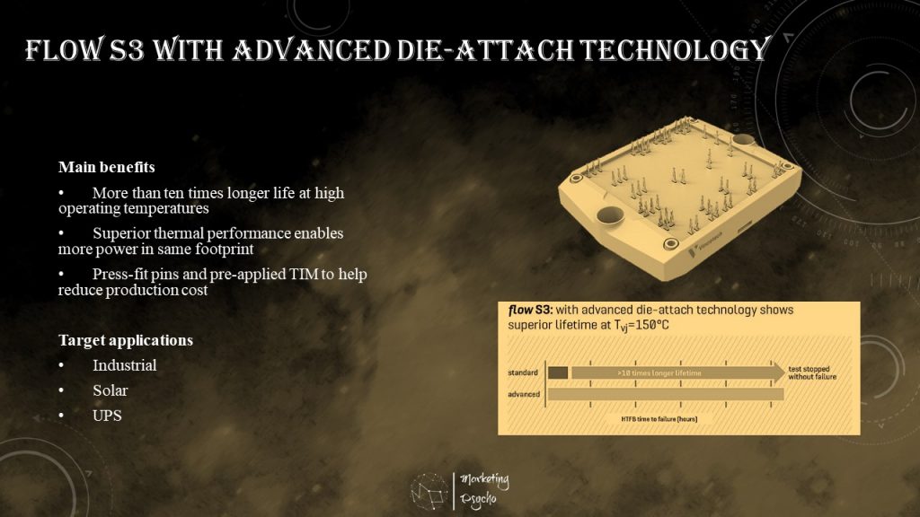
Flow S3 with Advanced Die-Attach Technology
More compact designs require greater power density, but reliability and service life are no less important to a product’s performance and reputation. Vincotech balances that equation with advanced die-attach tech and pre-applied phase-change material to extend lifetime and elevate power density. All flow S3 lines feature this leading-edge tech to bring both to customers’ products.
Main benefits
- More than ten times longer life at high operating temperatures
- Superior thermal performance enables more power in same footprint
- Press-fit pins and pre-applied TIM to help reduce production cost
Target applications
- Industrial
- Solar
- UPS
Zhixin Semiconductor Co., Ltd. IGBT Module Packaging and Testing Production Line was Officially Put into Operation
Dongfeng has taken an important step to independently control the key core technology resources of new energy vehicles. Starting this month, Dongfeng’s new energy passenger vehicles will be the first to be equipped with power semiconductor modules “Made in Wuhan”.
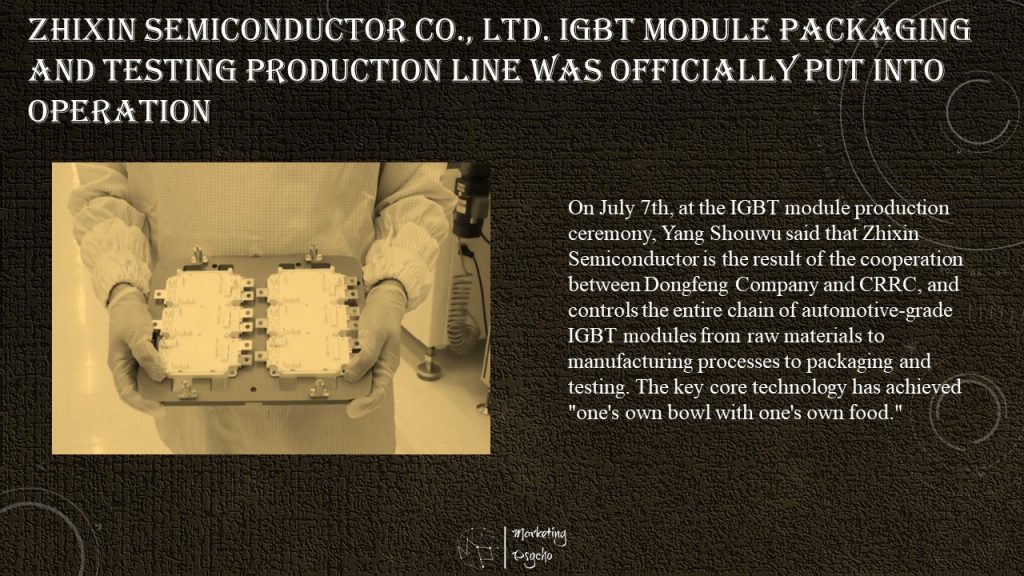
On July 7th, at the IGBT module production ceremony, Yang Shouwu said that Zhixin Semiconductor is the result of the cooperation between Dongfeng Company and CRRC, and controls the entire chain of automotive-grade IGBT modules from raw materials to manufacturing processes to packaging and testing. The key core technology has achieved “one’s own bowl with one’s own food.”
This automotive power semiconductor production line is based on the sixth-generation IGBT technology. It is currently the most advanced in China. The IGBT modules produced are safe, environmentally friendly, efficient, functional and quality comparable to imported similar products, and are at least 10 % cheaper.
The IGBT module production line officially put into operation on July 7 is only the first phase of Zhixin Semiconductor. It can produce 300,000 sets of IGBT modules per year and has a full set of IGBT design, manufacturing, packaging and testing capabilities.
“Dongfeng New Energy Automobile Industrial Park will become the first power semiconductor industrialization base in Central China.” Yang Shouwu said that the total planned production capacity of Zhixin Semiconductor is 1.2 million sets of IGBT modules. The demand for IGBT modules for the production and sales of 1 million new energy vehicles in 2025 can also be supplied to other car companies. Among them, the third phase of the project will develop and produce more advanced silicon carbide IGBT modules.
Li Donglin, chairman of CRRC Zhuzhou Electric Locomotive Research Institute Co., Ltd., said that Zhixin Semiconductor IGBT module products have the advantages of safety, environmental protection, and high efficiency. “With Zhixin Semiconductor IGBT products, domestic new energy automobile companies can not only further enhance the core competitiveness of products, but can also ensure the safety and control of the supply chain.”
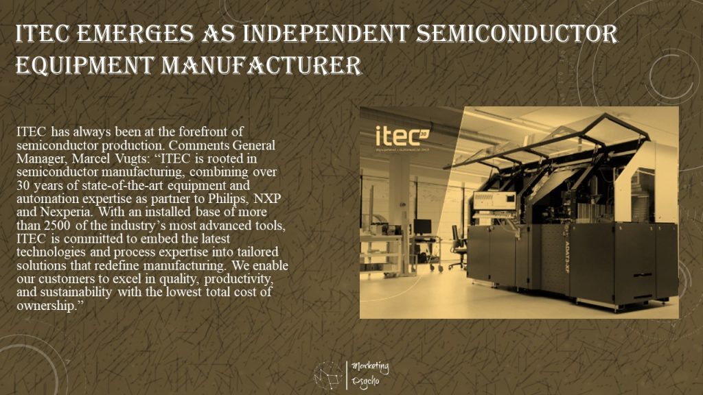
ITEC Emerges as Independent Semiconductor Equipment Manufacturer
ITEC, the semiconductor equipment manufacturer founded in 1991 by Philips (now Nexperia), announced its launch as a separate independent entity. ITEC remains part of the Nexperia group. This move will allow ITEC to address the third-party market in time to serve the current semiconductor boom. It provides manufacturers worldwide access to disruptive manufacturing solutions that are built to last.
ITEC has always been at the forefront of semiconductor production. Comments General Manager, Marcel Vugts: “ITEC is rooted in semiconductor manufacturing, combining over 30 years of state-of-the-art equipment and automation expertise as partner to Philips, NXP and Nexperia. With an installed base of more than 2500 of the industry’s most advanced tools, ITEC is committed to embed the latest technologies and process expertise into tailored solutions that redefine manufacturing. We enable our customers to excel in quality, productivity, and sustainability with the lowest total cost of ownership.”
Currently, ITEC offers the following benchmark solutions for best-in-class semiconductor back-end manufacturing:
- ADAT assembly equipment for die bond and chip sort – currently the fastest equipment of its type capable to process up to 20 dies per second, producing 1.5 million chips per system per day.
- Parset test platform – enables the electrical parameter testing of small signal and power MOS devices at a rate up to 92,000 chips per hour.
- Smart vision Inspection systems for semiconductor front-end and back-end manufacturing using deep learning technologies.
- Factory Automation and Smart manufacturing – complete equipment control software suite, combining scheduling, optimization, traceability and analysis functions using ‘Big Data’ analytics and machine learning to enable leading Industry 4.0 production for mass volume semiconductor manufacturing.
Vugts concludes: “During ITEC’s history, annual production of discrete semiconductors on our equipment has grown from 4.5 billion in 1991 to over 90 billion products in 2020 – that represents ten devices for every citizen on the world, each year. With the current worldwide shortage in semiconductors and lead times lengthening, ITEC – now as an independent company – is ideally positioned to support the exponentially growing industry, redefining the world of manufacturing.”
ASM Expands Its Epitaxy Product Offerings with New Intrepid® ESA™
ASM International N.V. introduced its Intrepid® ESA™ epitaxy tool for 300mm applications for power and analog devices, and for epitaxial silicon wafers. Based on the proven, high-volume-manufacturing Intrepid platform, the new ESA tool expands ASM’s atmospheric epi offerings with ASM’s first 300mm atmospheric cluster tool. The Intrepid ESA offers best-in-class on-wafer performance.
An expanding range of semiconductors are needed for 5G smartphones, internet of things (IoT), edge computing, automotive, sensors, renewable energy, and much more. ASM’s epitaxy tools are critical for depositing silicon-based films in diverse, fast growing applications for analog and power devices, as well as for silicon wafer manufacturing.
For chipmakers, the metrics that drive product yield and fab operational cost will be of utmost importance: the ability to manufacture a wide range of different products; on-wafer performance metrics, such as within-wafer and wafer-to-wafer uniformity; and productivity and foot print efficiency.
ASM has responded to this critical customer need with the introduction of the Intrepid ESA. The Intrepid ESA has innovative technologies and features that provide unmatched in-film performance and reactor availability. These include a hot quartz isothermal reactor for superior temperature uniformity, allowing for the deposition of films as thick as 85µm without interruption and reactor clean, a significant throughput and device performance benefit. Furthermore, ASM has introduced the first 10-port MFC-based advanced gas injection system, called AEGIS™, providing flexibility for film thickness profile control.
To further enhance device performance and die yield, ASM has pioneered real-time closed-loop wafer temperature control during epi processing allowing for the in-situ measurement and control of wafer temperature simultaneously in different areas of the wafer during processing. This first-of-its-kind feature enables the elimination of thermal gradient induced wafer slip in high temperature processing, resulting in improved die yield. In addition, Intrepid ESA can hold up to four reactors on its XP platform. It is compact in size, has dual gate valves for isolating each chamber with the XP platform, and has independent gas delivery systems.
These features enable considerably higher throughput and thus improved platform efficiency (wafer output per square meter) which we view as unique strengths of the Intrepid ESA.
“Innovative process control features such as AEGIS and closed loop chamber temperature control uniquely position Intrepid ESA as the best choice for our customers running applications for power and analog devices, and for wafer manufacturers,” said Dr. Hichem M’Saad, Executive Vice President and General Manager of ASM’s Global Products. “ASM strives to enable customers to scale cost effectively and with greater yield.”
More than 30 Intrepid ESA reactors, with repeat orders, are in production at different sites in Asia and the Unites States.
ST and Exagan, the New Chapter in the Gallium Nitride Story
Should engineers adopt Gallium Nitride (GaN) power devices, or is it still too early? Part of the answer lies in STMicroelectronics’ recent acquisition of a majority stake in Exagan, a French innovator with unique epitaxial growth expertise and one of a select few to enable the mass deployment and production of GaN power devices on 8-inch (200 mm) wafers. The investment in Exagan by ST is a continuation of their long-term commitment in compound power semiconductors. Indeed, ST recently launched MASTERGAN1, the first 600 V system-in-package with a gate driver and two enhancement-mode GaN transistors in a half-bridge topology. The device opens the door to cost-effective power supplies for laptops and smartphones, among other things. As a result, engineers are increasingly viewing the design and production of GaN power devices as mainstream.
Gallium Nitride is a compound III/V semiconductor material. It has a wide bandgap of 3.4 eV and an electron mobility of 1,700 cm2/Vs. Comparatively, Silicon sits at 1.1 eV and 1,400 cm2/Vs. GaN’s inherent properties thus result in a higher breakdown voltage and lower on-state resistance, which means that the component can more efficiently handle greater loads compared to a similar-sized silicon device, which then leads to a lower bill of materials. ST, seeing GaN’s potential, was one of the first companies to provide mainstream power devices featuring the new material. Indeed, the MASTERGAN series offers the first and only system-in-package in the industry with two e-Mode GaN transistors.
And now, the agreement with Exagan means ST will be the first company to have depletion-mode (D-mode) and enhancement-mode (E-mode) GaN devices in its portfolio. D-mode high electron mobility transistor (HEMT) use a “normally-on” die configuration, meaning that they have a naturally conducting channel that doesn’t require the application of a voltage at the gate. D-mode represents the natural form of GaN-based devices and it often integrates a low-voltage Silicon MOSFET in a Cascode configuration. On the other hand, “normally-off” or E-mode devices have a P-GaN channel that requires a voltage at the gate to be conductive. Both are increasingly present in consumer, industrial, telecom, and automotive applications.
Subscribe to Power Semiconductors Weekly and watch it on YouTube every Tuesday.
If you prefer a monthly update about the world of power semiconductors delivered to your e-mail address, please, subscribe to Marketing Psycho Power Semiconductors newsletter.