Power Semiconductors Weekly Vol. 21
Bosch Opens Chip Factory of the Future in Dresden
On June 7, 2021, under the tagline “The Future – Built by Bosch. #BoschSiliconDay,” wafer fab in Dresden was opened – one of the world’s most modern chip production facilities. At the same time, this is also the first AIoT factory. AIoT stands for the combination of artificial intelligence and the internet of things. Bosch is using it to make the plant in Dresden a fully connected, intelligent factory, thereby creating a sound basis for data-driven, continuous improvement in production.
Toshiba’s Triple-Gate IGBT Power Semiconductors Cut Switching Power Losses by 40.5%
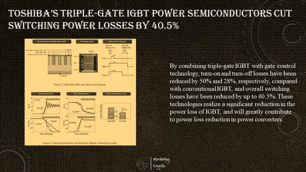
Toshiba Corporation has developed a prototype triple-gate IGBT that reduces overall power loss by up to 40.5% when switching on and off (switching losses), the process of allowing and stopping electricity flow, in power semiconductors used to control electric power.
It is difficult to reduce power loss in IGBT, due to a trade-off whereby reducing the loss when the IGBT is on (conduction losses) increases switching loss. Toshiba took on this problem by developing a silicon IGBT with a new structure of three gate electrodes and gate control technology that delivers high accuracy gate electrode switching. The new device reduces turn-on loss by 50% and turn-off loss by 28%, an overall reduction of up to 40.5% against a conventional single-gate electrode IGBT, with no increase in conduction losses.
Improving the energy efficiency of power semiconductors is seen as essential for realizing carbon neutrality, particularly by achieving higher efficiency IGBT, power semiconductors used in many products and equipment. The new technology is expected to boost the efficiency of power converters in electrical systems, including renewable energy systems, electric vehicles, railroads, and industrial equipment. Toshiba presented the technology at ISPSD2021.
Power semiconductors that control electric power flows are used in every aspect of power generation, transmission, storage and optimal use, and are crucial for ensuring power supply stability and reducing consumption. In recent years, the power semiconductor market has expanded with the increasing popularity of electric vehicles and the wider use of renewable energy sources, both steps toward the realization of a carbon-neutral economy. In October 2020, the Japanese government set the goal of achieving a carbon neutral Japan by 2050, and initiative like this are is expected to spur further market growth.
These developments are also driving efforts to improve power semiconductor performance, especially of IGBT, high-voltage power semiconductors installed in power converters in a wide range of electrical systems. Improving IGBT energy efficiency will greatly contributes to realizing carbon neutrality.
Conduction losses can be reduced by increasing the number of electrons and holes held on the device, but this increases switching losses. Silicon-based IGBT have been tweaked over the last 30 years by improving the structure to mitigate the trade-off between conduction losses and switching losses, but there have been no breakthroughs in recent years.
Toshiba has developed a triple-gate IGBT and gate control technology that significantly reduces switching loss through flexible control of the accumulation of electrons and holes, from the gate drive circuit side.
The three gates, the main gate (MG), primary control gate (CGp), and secondary control gate (CGs), can be driven independently. When gates are turned on, delaying CGs and first turning on MG and CGp ensures simultaneous large electron and hole flows from the three gate electrodes, and they accumulate in the IGBT at a higher speed, realizing a faster switching time and lower turn-on loss. When turning the gates off, electrons and holes inside the device are reduced by turning off CGp before MG, while leaving CGs off. When the MG is switched off, the IGBT switches off completely and the electrons and holes disappear at high speed, reducing turn-off loss.
By combining triple-gate IGBT with gate control technology, turn-on and turn-off losses have been reduced by 50% and 28%, respectively, compared with conventional IGBT, and overall switching losses have been reduced by up to 40.5%. These technologies realize a significant reduction in the power loss of IGBT, and will greatly contribute to power loss reduction in power converters.
5th Generation 650V SiC Schottky MPS™ Diodes for Best-in-Class Efficiency
GeneSiC Semiconductor, a pioneer and global supplier of Silicon Carbide (SiC) power semiconductor devices, announced the availability of 5th generation (GE*** series) SiC Schottky MPS™ rectifiers that are setting up a new benchmark with their superior price-performance index, industry-leading surge current and avalanche robustness, and high quality manufacturing.
Dr. Siddarth Sundaresan, Vice President of Technology at GeneSiC Semiconductor commented that “GeneSiC was one of the first SiC manufacturers to commercially supply SiC Schottky rectifiers in 2011. After more than a decade of supplying high-performance and high-quality SiC rectifiers in the industry, we are excited to release our 5th generation of SiC Schottky MPS™ (Merged-PiN-Schottky) diodes that offer industry-leading performance in all aspects to meet the high efficiency and power density goals in applications like server/telecom power supplies and battery chargers.
The revolutionary feature that makes GeneSiC 5th Generation (GE*** series) SiC Schottky MPS™ diodes stand out among its peers is the low built-in voltage (also known as knee-voltage); it enables lowest diode conduction losses at all load conditions – crucial for applications demanding high-efficiency energy usage. In contrast to other competitor GeneSiC SiC diodes also designed to offer low-knee characteristics, an additional feature of GeneSiC Gen5 diode designs is that they still maintain that high level of avalanche (UIL) ruggedness that our customers have come to expect from GeneSiC’s Gen3 (GC*** series) and Gen4 (GD*** series) SiC Schottky MPS™”
Features:
- Low Built-In Voltage – Lowest Conduction Losses for All Load Conditions
- Superior Figure of Merit – QC x VF
- Optimal Price Performance
- Enhanced Surge Current Capability
- 100% Avalanche (UIL) Tested
- Low Thermal Resistance for Cooler Operation
- Zero Forward and Reverse Recovery
- Temperature Independent Fast Switching
- Positive Temperature Coefficient of VF
Applications:
- Boost Diode in Power Factor Correction (PFC)
- Server and Telecom Power Supplies
- Solar Inverters
- Uninterruptible Power Supplies (UPS)
- Battery Chargers
- Freewheeling / Anti-parallel Diode in Inverters
G3R™ 750V SiC MOSFETs Offer Unparalleled Performance and Reliability
GeneSiC’s next-generation 750V G3R™SiC MOSFETs will deliver unprecedented levels of performance, robustness and quality that exceeds its counterparts. System benefits include low on-state drops at operating temperatures, faster switching speeds, increased power density, minimal ringing (low EMI) and compact system size. GeneSiC’s G3R™, offered in optimized low-inductance discrete packages (SMD and through hole), are optimized to operate with lowest power losses under all operating conditions and ultra-fast switching speeds. These devices have substantially better performance levels as compared to contemporary SiC MOSFETs.

Dr. Ranbir Singh, President at GeneSiC Semiconductor commented that “high-efficiency energy usage has become a critical deliverable in next-generation power converters and SiC power devices continue to be the key components driving this revolution. After years of development work towards achieving the lowest on-state resistance and robust short circuit and avalanche performance, we are excited to release the industry’s best performing GeneSiC 750V SiC MOSFETs. GeneSiC G3R™ enable power electronics designers to meet the challenging efficiency, power density and quality goals in applications like solar inverters, EV on-board chargers and server/telecom power supplies. An assured quality, supported by fast turn-around and automotive-qualified high-volume manufacturing further enhances their value proposition.”
Features:
- Industry’s lowest gate charge (QG) and internal gate resistance (RG(INT))
- Lowest RDS(ON) change with temperature
- Low output capacitance (COSS) and miler capacitance (CGD)
- 100% avalanche (UIL) tested during production
- Industry-leading short circuit withstand capability
- Fast and reliable body diode with low VF and low QRR
- High and stable gate threshold voltage (VTH) across all temperature and drain-bias conditions
- Advanced packaging technology for lower thermal resistance and lower ringing
- Manufacturing uniformity of RDS(ON), VTH and breakdown voltage (BV)
- Comprehensive product portfolio and safer supply chain with automotive-qualified high volume manufacturing
Applications:
- Solar (PV) Inverters
- EV / HEV Onboard Chargers
- Server & Telecom Power Supplies
- Uninterruptible Power Supplies (UPS)
- DC-DC Converters
- Switched Mode Power Supplies (SMPS)
- Energy Storage and Battery Charging
- Induction Heating
Japan Puts All Chips on the Table to Lure Semiconductor Makers
Japan will pull out every policy stop to court overseas semiconductor companies, including offering generous financial incentives, under a draft growth strategy, joining the global race to secure supplies of the crucial component.
“Japan will swiftly match efforts by other countries to attract cutting-edge chipmaking facilities so it can build a secure supply chain at home,” said the document presented to a Cabinet Office strategy meeting. The Cabinet is slated to approve the document by the end of the month.
Japan imports more than 60% of its semiconductors, much of them from Taiwan and China. Concerns persist that Sino-American tensions could squeeze global supply chains and disrupt shipments to its own industries.
This comes as the U.S. and Europe make aggressive moves to bolster their own supply chains of semiconductors, which are increasingly seen as critical to economic national security. Japan hopes to sweeten financial incentives, but matching the financial power of the U.S. or the European Union will be a challenge.
“Semiconductors are now as important as food or energy,” an official at Japan’s Ministry of Economy, Trade and Industry said.
“We will aim for cooperation with foreign companies instead of efforts by Japanese players alone,” a Cabinet Office official said.
Some in the government and the ruling Liberal Democratic Party are calling for the creation of a new supersized fund worth tens of billions of dollars. Debate over the details is expected to get underway soon.
The U.S. Innovation and Competition Act, which is currently in the Senate, would allocate $39 billion over five years to assist chipmakers that build factories and research facilities in the U.S.
The EU plans to invest 145 billion euros ($177 billion) into digital technologies, including semiconductors, over the next two to three years. Japan also has a fund designed to promote advancements in the industry, but it is relatively small at 200 billion yen ($1.82 billion).
Subscribe to Power Semiconductors Weekly and watch it on YouTube every Tuesday.
If you prefer a monthly update about the world of power semiconductors delivered to your e-mail address, please, subscribe to Marketing Psycho Power Semiconductors newsletter.