Power Semiconductors Weekly Vol. 14
I-VI Incorporated Expands Silicon Carbide Manufacturing Footprint for Power Electronics in Electric Vehicles and Clean Energy Applications
II-VI Incorporated, a leader in wide-bandgap compound semiconductors, announced that it has expanded its silicon carbide (SiC) wafer finishing manufacturing footprint in China to serve the largest worldwide market for electric vehicles (EVs) and for clean energy applications.
Spurred by increasing regulatory requirements for lower emissions of greenhouse gases and the decreasing cost of lithium-ion batteries, the market for electric vehicles is growing rapidly and driving the demand for power electronics that are based on silicon carbide, a wide-bandgap material that increases the driving range of electric vehicles by about 10% on a single charge, compared with power electronics based on silicon. To meet the market demand in Asia, II-VI has established a backend processing line for conductive SiC substrates, in over 50,000 sq. ft. of new cleanroom space, at II-VI’s Asia Regional Headquarters in Fuzhou, China.
“According to recent industry reports, China is expected to continue to be the world’s largest electric car market at over 40% of global sales,” said Sohail Khan, Executive Vice President, New Ventures & Wide-Bandgap Electronics Technologies Business Unit. “We are planning to substantially increase our global production capacity for SiC boules and substrates in the U.S. over the next 5 to 10 years to address the accelerating power electronics market, including for electric vehicles and clean energy applications. These investments will be supported by our global sales force and a SiC platform built by our innovations of the last 20 years, including the world’s first 200 mm conductive substrates in 2015. We are excited about our prospects to lead in one of the most promising markets of our generation.”
In addition to electric vehicles, power electronics based on SiC enable high efficiency in inverters for solar and wind energy generation, as well as in smart-grid power switching, due to reduced switching losses, high power density, better heat dissipation, and increased bandwidth capability, compared with existing devices based on silicon.
New LoPak module: Now for 1200 V Applications with Same Familiar Packaging
Building on its experience of high-performance, high-reliability devices for voltages above 3.3 kV, Hitachi ABB Power Grids has expanded its product portfolio by introducing a family of 1200 V power modules to complement the existing 1700 V family, starting with a 1200 V, 900 A x 2 module using an upgraded LoPak module package.
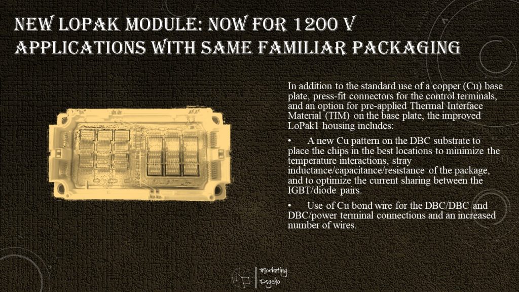
In addition to the standard use of a copper (Cu) base plate, press-fit connectors for the control terminals, and an option for pre-applied Thermal Interface Material (TIM) on the base plate, the improved LoPak1 housing includes:
- A new Cu pattern on the DBC substrate to place the chips in the best locations to minimize the temperature interactions, stray inductance/capacitance/resistance of the package, and to optimize the current sharing between the IGBT/diode pairs.
- Use of Cu bond wire for the DBC/DBC and DBC/power terminal connections and an increased number of wires.
Read more about it in the upcoming May issue of Bodo’s Power Systems!
IIT Hyderabad, NXP India, MeitY Join Hands to Boost Semiconductor and IP Startups
IIT Hyderabad, Ministry of Electronics and IT (MeitY) and NXP India have joined hands to announce the launch of the first ‘Semiconductor Startup Incubation and Acceleration Program’.
The program aims to locate, facilitate, and mentor semiconductor and IP design start-ups in India in both, technological as well as business aspects.
NXP India is among the biggest R&D centers for NXP Semiconductors and a world leader in secure connectivity solutions for embedded applications.
As per a statement, the program will support India’s vision of making the country a self-reliant nation as it creates a ready platform to support start-ups who wish to design semiconductor chips in India.
The local hardware designing and manufacturing of products will strengthen the core Technology-driven System pillar vision of Aatmanirbhar Bharat and in turn will boost India’s economy, generate employment, and enhance India’s position globally in the electronics industry by moving up in the value chain, the statement added.
TSMC Plant Hit By Power Outage – Millions Of Dollars In Damage Expected
The Taiwan Semiconductor Manufacturing Company’s (TSMC) chip fabrication plant in the province’s Tainan sector experienced a power outage. This facility is responsible for fabricating semiconductors on the 12nm and higher process nodes, with its output primarily used to supply chips destined for automotive uses. It comes as the global automotive industry is dealing with a semiconductor supply crisis, and initial, unofficial estimates suggest that the damage could amount to millions of NT$.
Due to the outage, Taiwanese industry sources expect that the damage to TSMC’s output can reach millions of NT$. While the company is yet to officially provide an update about the damage, up to 30,000 wafers are expected to be impacted due to the power breakdown.
The P7 plant in the 14B factory in the center of the outbreak is believed to have a monthly production capacity of 40,000. Judging by this, the 30,000 wafer loss estimate seems to be exaggerated. Therefore, it should not be taken as set in stone unless further details on the matter come to light.
Bidirectional Topologies and Semiconductors for e-Mobility On-Board Chargers
Implementing bidirectional power flow capability in on-board chargers has an impact on the choice of topology and power semiconductor technology for designers. The complete chipset, including sense, supply and control, also needs to be considered to ensure the best possible system solution.
Grid blackouts often happen after natural disasters and weather events. Bidirectional power flow in xEVs enable people to run key home appliances such as refrigerators, ovens and lights for a number of days until the AC grid is re-established. Furthermore, xEVs equipped with bidirectional power flow can help stabilize and reinforce the AC grid during peak power demands and provide an additional source of electricity for the local AC grid provider.
This presentation looks at the regulations that are currently being considered for the bidirectional operation of on-board chargers in hybrid, plug-in hybrid and fuel-cell electric vehicles (xEV). It provides an overview of bidirectional capabilities in the market today and the trends in the near to mid-future.
Attendees will learn about the different bidirectional topologies used in on-board chargers. They will also understand which power semiconductor technologies are appropriate for each topology and discover the various complementary devices, such as gate drivers and microcontrollers, that feature in chipsets for electromobility applications.
Key Takeaways
- Learn about the regulations governing bidirectional power flow in xEVs and how they affect the choice of topologies and semiconductors.
- Discover which xEV designs require bidirectional power flow and the reasons behind this.
- Understand the different bidirectional topologies in on-board chargers (OBC) and the DC-DC converters that can be used to best enable this feature.
- Find out how Infineon semiconductors enable bidirectional power flow in xEVs and meet the demands of this trending feature.
- Learn more about the on-board charger solutions and additional helpful resources offered by Infineon.
Find more information about power semiconductors in Marketing in Power Electronics section of the website.